|
OPTO COUPLERS |
OPTO-COUPLERS are also called OPTO-ISOLATORS or PHOTO-COUPLERS.
An opto-coupler is an optical link and it connects two circuits via this link.
The optical link is contained within a chip. A Light Emitting Diode inside the chip shines on a photo-diode, photo-transistor or other photo device.
When the photo device sees illumination, the resistance between its terminals reduces. This reduced resistance can activate another circuit. See this in operation in the animation below.
An opto-coupler is designed to withstand a very high voltage (500v to 10kv) between its input and output. This is called ISOLATION. It can also be called INSULATION, but the term isolation is used more frequently.
The other main advantage of an opto-coupler is the ability to have the input and output at different potentials. This is also called isolation but it means the two circuits can have different "earth rails" or 0v rails.
GENERAL DETAILS:
All opto-couplers have the same feature - a circuit activates another circuit via an optical link - passing information from one circuit to another.
There are a number of differences between opto-couplers. Some have a transistor, triac or Schmitt Trigger output, some have high isolation and others have a high speed of operation. Some will transmit audio and digital information, other will only transmit digital information.
Transistor versions can be used to transmit digital or audio information.
When deciding on an opto-coupler, here are the 5 steps:
1. Start with isolation voltage. Do you need 500v isolation or 2kv?
2. Check type of output. Do you want to pass audio or digital information?
3. Check speed of operation. Do you need high speed?
4. Check availability
5. Check price
Nearly all opto-couplers have the following features:
Between 1mA and 15mA is needed to illuminate the LED.
The transistor in a photo-transistor type is capable of withstanding 20v - 70v.
Photo-thyristor types are capable of withstanding 250v - 400v.
For high-speed operation a NAND gate version is available.
HOW AN OPTO-COUPLER WORKS:
(this is a theoretical circuit - see below for a practical circuit)
between the collector and emitter of the
transistor DECREASES.
The voltage on the output REDUCES
The animation above shows an opto-coupler in operation.
The LED requires 1mA to 15mA.
What does this mean?
If the current-limiting resistor connected to the LED has a high value,
only a small current will flow through the LED and it will not glow very
brightly. (The LED is inside the chip - you cannot see it).
The transistor will not turn on very much and the resistance between the
collector-emitter terminals will be fairly HIGH. The output voltage will
remain fairly HIGH.
As the current through the LED increases, (the current-limiting resistor
is reduced in value) the LED will glow brighter and the transistor will
turn on harder. The output voltage in the diagram above will reduce.
If the current through the LED is allowed to rise and fall, the output
voltage of the circuit above will fall and rise. In this way the
opto-coupler will pass AUDIO.
If the current through the LED changes instantly from zero to say
15mA, the output will change from HIGH to LOW. This is the principle of
SWITCHING or passing a DIGITAL SIGNAL.
The output transistor will pass 30mA to 100mA.
What does this mean?
For instance, you cannot put a 12v @ 1amp globe on the output of
the opto-coupler. It will not illuminate. However a 12v @100mA relay can be placed on the output will
operate.
To get an output signal from an opto-coupler when it is placed as shown
in the circuit above, you need to place a
resistor on the collector-lead. This is called a "LOAD RESISTOR"
or "PULL-UP RESISTOR." When the opto-coupler is
producing a LOW, the load resistor is passing a current called "wasted current."
An improved circuit is shown below:
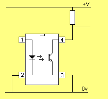
When the photo-transistor in the opto-coupler above is
not detecting illumination, it has a high resistance between pins 3 and
4. We can say the output is LOW (this is not technically correct, but
will be ok for this discussion).
When the photo-transistor detects illumination, the resistance between
pins 3 and 4 is small and we can say the output is HIGH.
A resistor is needed on the output of the opto-coupler to prevent
damaging the transistor.
The value of this resistor is determined by one of the following:
1. The maximum current-flow is less than 100mA for a 100mA transistor
etc.
2. The current-flow should be sufficient to drive the circuit connected
to the opto-coupler.
The
resistor on the output is called a "current-limiting" resistor. It should
be chosen to allow about 200% - 300% more current than that required by
the stage it is driving.
This allowance is needed as some transistors have a
spread of parameters and may have a lower gain than the "test
circuit."
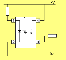
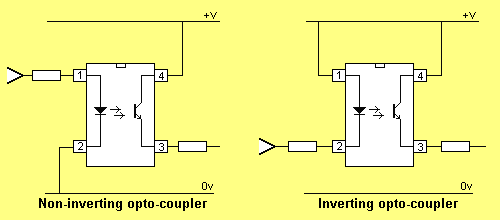
An opto-coupler can invert a signal or provide non-inversion.
The diagram below shows the two arrangements:
COMPLETE RANGE:
A complete range of opto-couplers is available from: ISOCOM Ltd OPTOCOUPLERS.
See their complete list with parameters for each device.
Click: pinouts to link to all optocouplers having that pinout!
Here are a few common optocouplers:
| Device | Vce |
Viso |
Pinout |
|
H11A1 4N25 4N28 5FH601 6N138 MOC3031 MOC3010 4N33 TIL111 MOC223 H11C5 H11D1 CNY17-1 THCC240 |
30 |
7k5 |
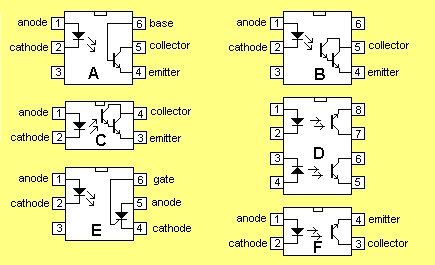
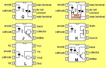
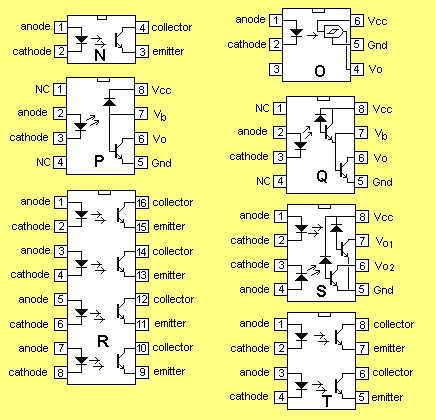
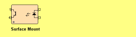
The diagrams below show the range of layouts for opto-couplers:
 |
 |
 |
 |