|
|
BASIC
ELECTRONICS COURSE
Page 29
 INDEX
INDEX
There is one more
GATE we need to cover. It is the . . .
THE
SCHMITT TRIGGER INVERTER
The SCHMITT TRIGGER INVERTER is an INVERTER with a SCHMITT TRIGGER input.
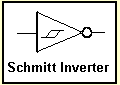
It is basically a GATE and can be used as an INVERTER. But the
Schmitt Trigger input gives it a lot more features.
The Schmitt Trigger Inverter is shown on the left and the
Schmitt symbol must be included to show it is not an ordinary
inverter.
This is a very useful BUILDING BLOCK and can be used in many
different ways.
It can be used as an Inverter, an oscillator, a Buffer as well as
other "Building Blocks." It all depends on the surrounding
components.
When you add components to create a circuit that performs a
"function," the result is called a BLOCK, or BUILDING
BLOCK or STAGE.
There are 6 Schmitt Inverters in the chips we will be discussing
and this allows 6
separate "stages" or "blocks" to be
produced. That's why complete projects can be designed around
a single chip.
When wired as an oscillator, only two
external components are needed. If you require the oscillator to
be turned on and off, a low-frequency oscillator can gate the
oscillator (as shown previously). If you require the oscillator
to drive an output device, two Schmitt Inverters can be wired in
parallel to deliver the drive-current. If you require a
load but WITHOUT inversion, two Schmitt gates can be placed in
series. (This is called "double inversion" and is
equivalent to a BUFFER.)
The chip we are referring to is the HEX SCHMITT TRIGGER with the
basic identification of 74C14.
This chip is also known as 40106 or 74F14 or
74HC14. They are all pin-for-pin compatible devices. The
advantage of the 74HC14 is it will operate on a voltage as low
as 3v.
The range of
circuits you can design with this chip is endless but before
you can start designing, there are two features we need to
cover.
1. The Hysteresis of
a Schmitt Trigger
2. The Time Delay Circuit.
1.
THE HYSTERESIS OF A SCHMITT TRIGGER
The Hysteresis of
a Schmitt Trigger is the gap between the low point where the
gate changes state and the high point. This gap is typically 33%
of rail voltage and because this gap is so wide, it is very
difficult for noise to enter the gate and cause false
triggering. This makes the gate ideal for noisy situations but
it will not amplify low-level signals and therefore cannot be
used where small signals are required to be amplified. This is
the only drawback of a Schmitt Trigger.
The hysteresis is
the "dead gap" between 33% and 66% of rail voltage and
these two levels are discussed fully below.
2.
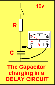
THE TIME DELAY CIRCUIT
The time delay circuit is also know as a "TIMING CIRCUIT," "DELAY
CIRCUIT," or "R-C
CIRCUIT".
These names all refer to a CAPACITOR and RESISTOR in
series. It does not matter if the capacitor is placed above or below
the resistor as the time delay will be the
same. The only difference
will be the value of the voltage at the beginning and end of the timing
cycle.
If the capacitor is above the resistor, as shown in the first diagram
below,
the voltage will RISE from zero to rail voltage.
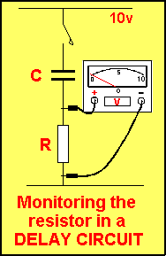
If the capacitor is below the resistor, as shown in the second diagram,
the voltage will fall from rail voltage to zero.
The join of the two components is the point where the voltage is
detected and is called the "Detection Point."
The Detection Point is monitored by a Detection Circuit.
This can be any of the gates we
have described or a transistor or a multimeter.
The detection circuit must not load the timing
circuit. In other words the detection circuit must have a very
high input impedance and as we have already described, CMOS
gates have a very high input impedance. That's why they are
ideal for detecting the voltage on a DELAY CIRCUIT.
When voltage is
applied to a TIMING CIRCUIT, the capacitor begins to charge. If
we monitor the voltage across the capacitor, we can determine
when it is at a particular voltage level. It will take a
PERIOD OF TIME to reach this level and this is the TIME DELAY we
require.
In the animation below we see the capacitor charging via a
resistor, with a meter showing the approx voltage across the
capacitor. We have already mentioned the capacitor does not
charge at a constant rate, but this characteristic does not
concern us at the moment.
The point to remember is the TIME it takes for the capacitor to
charge.
In the animation
below, the meter is monitoring the voltage across the RESISTOR.
As you can see, the voltage across it is falling as the
capacitor charges.
As the voltage across the capacitor
INCREASES, the voltage across the resistor DECREASES because the
total voltage across the combination is 10v, and the voltage
across each must add up to 10v.
If we connect the
DELAY CIRCUIT to the output of a gate (any gate can be used -
but we will choose an INVERTER and since we are discussing the
Schmitt Inverter, we will use it) we can CHARGE the
capacitor when the output of the Schmitt Inverter is HIGH
and DISCHARGE the capacitor when the output is LOW.
The animation below shows how the voltage across the capacitor
rises and falls during the cycle. The actual shape of the graph
does not concern us. We are only interested in VOLTAGE LEVELS
and the TIME TAKEN for the voltage to rise and fall.
We will discuss the voltage levels in a moment. For the moment
you need to know the levels detected by a SCHMITT
INVERTER are: 33% and 66% of rail voltage. These two levels are
shown on the graph.
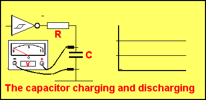
Here comes the
clever part. Instead of the voltmeter monitoring the voltage
across the capacitor, the input of the Schmitt Inverter can be
connected to the capacitor.
If the voltage across the capacitor is less than 66% of rail
voltage, the output of the gate is HIGH and the capacitor begins
to charge. When the voltage reaches 67%, the output goes LOW and
the capacitor begins to discharge. When the voltage across it
reaches 32% of rail voltage, the Schmitt Inverter changes state
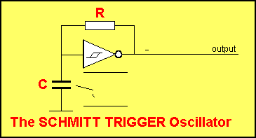
and the output goes HIGH. In this way we need only one gate to create an oscillator.
There are two very important things to observe in the animation
below.
1. The output is a square wave. In other words the output goes
from one state to the other VERY QUICKLY and this
produces the characteristic waveshape.
2. The voltage across the capacitor is EXACTLY 32% to 67% of
rail voltage.
The
animation below shows the gate in operation.
You will notice that the diagram does not show the chip
connected to the positive and negative rail. It is ASSUMED
the chip is connected to the supply voltage and that's how the
output produces the HIGH.
A point to remember:
1. The output of the chip is always the reverse (opposite) of
the input. The chip INVERTS the level (HIGH or LOW) on
the input and makes the output the OPPOSITE.
If the Input is HIGH, the output will be LOW
etc.
HOW
THE SCHMITT OSCILLATOR WORKS
Suppose the input is LOW. The output will be HIGH. The voltage
across the resistor will cause current to flow through it and
charge the capacitor. When the voltage on the capacitor reaches
67% of rail voltage, the gate will change state.
The energy in the capacitor will "bleed" through the
resistor and the voltage across the capacitor will gradually
fall. When it reaches 32% of rail voltage, the gate will change
state.
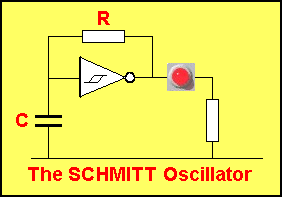
By selecting the
correct values for R and C, the Schmitt Oscillator can flash an
LED at a low flash rate. The 470R resistor in series with the LED
has nothing to do with the flash rate. It must be included
so that the output of the gate goes HIGH. If it is omitted,
the output will not rise above 1.7v. This is the characteristic
voltage across a LED and has been discussed in the first pages
of this course. If the resistor is reduced in resistance, it
will load the output and the output will not rise to rail voltage. If
this occurs, the input will not see 67% of rail voltage and the
gate will not change state.
The output of a 74C14 Schmitt gate will deliver about 15 - 20mA.
If the load requires more than about 20mA, a buffer (driver)
transistor will be needed. The output will deliver
more than 20mA but the output will not be full rail voltage. A
small drop will not affect the performance of the oscillator,
but if the load current is increased, a
point will come when the output will not rise to 67% of rail voltage
and the input will not allow the gate to change state.
|