THE
CURRENT THROUGH EACH STAGE
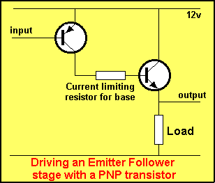
The current to drive the output transistor in the circuit below
is controlled by the current flowing into the base. This current
comes from the PNP transistor and base resistor.
The resistor limits the current through the base to prevent the
transistor being damaged. In other words, if the PNP
transistor tries to allow too much current to flow in the base, the resistor will limit
it to a safe
value.
The LOAD is shown as a load resistor in the
circuit. This is the conventional way to show a LOAD. It can be a globe, motor or relay and
for an EMITTER FOLLOWER stage. It is placed between
the emitter and negative rail. The word "output" has
been included on the diagram as the emitter lead is called the
"output." For an EMITTER FOLLOWER, you have to
remember the output is actually between the emitter and negative
rail.
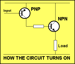
To show how this circuit works, we have included 2 animations:
"click 1" "click 2"
Click1 refers to the PNP transistor
Click2 refers to the NPN transistor
So far we have shown
how the current increases through the load as the current
increases into
the base of the PNP transistor. The transistors are CURRENT AMPLIFIERS.
But this is only half the explanation.
There is another way to describe the operation of the circuit.
It explains the circuit from the stand-point of
voltages.
As the voltage between base and emitter of the PNP transistor
increases, (in this case, the voltage on the base moves in a
downward direction so
that the effective voltage between base and emitter increases)
the transistor turns on MORE and this causes the voltage on the
base of the NPN transistor to INCREASE.
In other words the base RISES and takes the emitter with
it.
The emitter delivers a higher voltage to the load and whenever a
higher voltage is applied to a device, a higher current is
required. The NPN transistor is capable of delivering this
higher current via the collector-emitter leads and the circuit operates successfully.
The voltage across the load will range from 0v to about 1v less
than rail voltage. The animation below shows the load receiving
a voltage as the PNP and NPN transistors turn ON.
In the animation above, the voltage on the base of the PNP
transistor is falling but this is actually a TURN-ON voltage as
far as the transistor is concerned. In other words the PNP
transistor is TURNING-ON. The voltage on the base of the NPN
transistor rises and this RAISES the NPN transistor. The voltage
on the emitter of the NPN transistor INCREASES and thus the
voltage on the load INCREASES.
The
point is this: you have to consider the operation of the circuit in terms of VOLTAGE as well as CURRENT to get
the full picture.
In the circuit above, you can see how a higher voltage is
delivered to the load when the voltage on the PNP transistor is
altered.
To turn the PNP transistor on MORE, you must deliver more
current to its base and the voltage between base and emitter
increases slightly up to a maximum of about 0.75v. The resistance
between the collector-emitter leads of the PNP transistor
decreases and this allows current to flow into the base of the
NPN transistor.
The NPN transistor increases the
current through its collector-emitter terminals and also through the LOAD.
We are covering this action is detail because you have to be able
to VISUALISE the operation of the circuit if you want to design a
project.
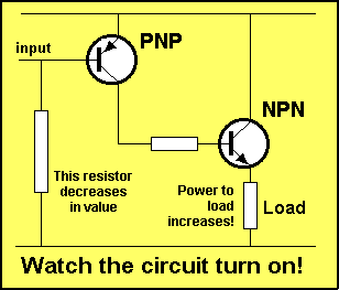
Here's one more animation to help you see how it works: The
circuit below shows the current into the base of the PNP transistor
increasing due to the resistor between base and 0v rail decreasing
in value. This is shown by the symbol getting shorter. As the
resistor decreases in resistance, the current into the base of the
PNP transistor increases and both the voltage and current
INCREASES to the load. In other words, the POWER to the load
increases.
The first resistor can be replaced with a transistor (creating a
3-transistor circuit). When the
transistor turns on, its resistance decreases, just like the
resistor in the animation.
Electronics Engineers "see" circuits working just like
the one above. That's how they can design and/or fault-find a
circuit.
If a circuit is not working, the engineer needs to know how the
circuit is laid-out in broad terms and how each stage is
connected together. It's very important to know if the stages are
"AC coupled" (capacitor coupled) or DC coupled (directly
coupled - the letters DC actually mean Direct Current).
It's important to know if the transistors are PNP or NPN and if
each stage is Common Emitter, Common Collector or Common
Base.
A circuit diagram will identify all these details and then it's a
matter of "seeing" how the stages work. If a circuit
diagram is not available, the engineer needs to trace out the
diagram so he can diagnose it correctly.
Animations are very helpful in presenting the
operation of a circuit. They help you see what the engineer sees
when he is diagnosing a problem. When you get to the stage of
being able to "see" a circuit working - you are half-way
there!
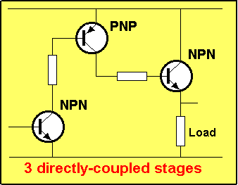
In the diagram below, the first transistor (an NPN transistor) is
turning on and driving the two stages we have been studying
previously. This makes the circuit a 3-stage DC (directly coupled)
arrangement.
DC
COUPLING
DC coupling produces enormous amplification and since the gain
(and operating conditions) of a transistor change according to the
temperature of the circuit, a DC arrangement is quite often
difficult to stabilize. This is a point to remember and that's why
it is almost impossible to directly couple more than 4 stages
together without providing a form of feedback called STABILIZATION. This is effectively a form of negative
feedback.
The resistor we have added to the circuit limits the current into
the base of the PNP transistor. It is necessary because the first
transistor can reduce to a very small value of resistance and this
will cause too much current to flow into the base of the PNP
transistor and possibly damage it.
TURNING
THE CIRCUIT
ON
It is important to
know how the circuit above turns ON. The voltage on the base of
the first NPN transistor must be above 0.6v for the transistor
to begin to conduct. Below this value, all the transistors are
turned OFF.
As the voltage on the base rises above 0.6v, the effective
resistance between the collector and emitter terminals DECREASES and this turns on the other two
transistors.
What you are actually doing is delivering a slightly higher
current to the base of the first transistor and the
characteristic of the transistor is to allow the voltage on its
base to rise to about 0.75v
In other words we can detect
the voltage on the base via a very sensitive multimeter set to
low volts and this is our simple way of detecting the
"state-of-turn-on" for the transistor.
At this level the transistor is fully turned ON. This will fully
turn on the other two transistors and the voltage on the load
will be very nearly rail voltage. [This will only be the case if
the third transistor is capable of delivering the current
required by the load. If the transistor is not capable of
delivering the current, the voltage across the load
will be less than expected - that's one of the realities of the
circuit that you only find out when you put it into
operation!]