|
|

Chapter 3
P1 P2
P3
Disassembler
START
HERE
Soldering and using a prototype PC
board
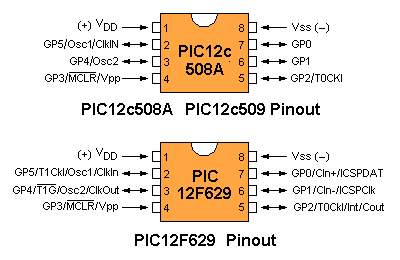
PIC12F629 Data
Sheet (.pdf 4,926KB)
PIC12c508A Data
Sheet (.pdf 1,600KB)
Instruction Set for PIC12F629
blank12F629.asm
template
Notepad2.zip
Notepad2.exe
PIC12F629.asm Chip as a "D" flip flop
Programming and using the surface Mount version
Library of Sub-routines "Cut and Paste"
Library of routines:
A-E
E-P
P-Z
PIC12F629 Project: 2-Digit Counter
PIC12F629 Project:
20 LED Display-1
10 Projects using
the PIC12F629
12 FREE PIC Books Simply download the books via Rapidshare.
Lots of PIC micro information on
this
website.
![]()
You may be asking "Why do I use a PIC chip?" The
answer is simple. There is nothing else.
Let me fill you in. I have been developing a range of modules similar to the
talking modules and music chips in greeting cards. But these "sound" cards
are so prosaic. The tunes are frightful and the speech is quite unfunny.
For a person like me, who has never bought a card in his life, it is unusual to
be designing electronic cards.
Possibly because most of the cards on the market "fall between two stools," I
have decided to design something that is a pleasure to give.
I don't like gaudy, over-designed images or wording that doesn't fit the
occasion. For that reason the cards I have designed are simple and uncluttered.
But more important, they contain an electronics module that delivers a concept
that has never been produced.
For a few extra dollars you get a card that contains a gift that can keep the
recipient happy for the afternoon.
Some of the ideas for the modules include a Reaction Timer, a "sky writer that
produces words in the air, a 20 second timer, a game of NIM and a
decision-maker.
All the circuits are designed around an 8-pin microcontroller - the PIC12F629.
At first glance this chip seems to be too expensive, at about 60 cents, and I
was steered in the direction of the ATMIL TTtiny11. But it was soon realised
this chip was going out of production and the ATtiny12 was heading the same way.
The next chip in the range was ATtiny13 but the cost was higher than the PIC
chip and I would have to transport my code as well as suffer a slightly reduced
output drive current.
Then MicroChip came to the rescue with a special chip for production-runs. Not
only was it cheaper but it had additional features above the PIC12F629. The only
reductions on the '629 are 2-stack (instead of 8), fewer registers and in
different locations (that's why you use the "equ" statement), and no EEPROM (so
data is lost when the chip is turned off). But the plus-values include an
Analogue to Digital Converter and a precision voltage reference.
I also tried all the other manufacturers and nothing similar in price was
available.
So, the decision is made and the supply is guaranteed for quantities of 100,000.
If you are thinking of designing anything for the mass-market, email me before
starting anything so you don't waste time searching in the wrong direction as
there are chips that are not available to the consumer market.
Before reading this article, go to
ICP article. It shows how to
solder a surface-mount or through-hole PIC12F629 to a PC board with a
programming socket that will accept In-Circuit Programming. Use the kit
on the ICP page to write your first program. The article also shows how to use
the PICkit-2 USB programmer.
|

Before we start: If you don't
know the state of some of the bits (or don't want to alter them - by
mistake), you can use the XOR instruction.
Although the PIC12F629 is
an up-grade of the PIC12C508 and '509, the program from a PIC12C508 cannot be
transferred directly to a PIC12F629 as there are a number of differences between
the two chips. The following items cover some of the differences.
1. The CALL Instruction
The CALL instruction for a PIC12C508,9 only works to the first 256
locations.
The CALL instruction
for a PIC12F629 accesses ALL MEMORY.
2. The
STACK
The PIC12C508A has only a 2-CALL stack.
The PIC12F629 has an 8-CALL stack. (8-level stack).
3. The In/Out Port
The IN/OUT port on a PIC12F629
is file 05h.
This port corresponds to pins 7, 6, 5, 4, 3, and 2 for GP0, GP1, GP2,
GP3 GP4 and GP5.
Remember: GPIO,3 (GP3) (pin 4) is an INPUT-ONLY pin.
When writing a program, use GPIO,0 GPIO,1 GPIO,2 GPIO,3 GPIO,4 GPIO,5 in
your program and the compiler will do the rest. (GPIO = General Purpose
Input/Output).
For instance, If you want to SET (make HIGH) pin 7, you must do
two things:
1. Make sure GPIO,0 is an OUTPUT bit by making the corresponding bit in
the TRISIO register "0." This is done via the following
instructions: Remember: "0" = output, "1" = input
bsf
status, rp0 ;bank 1
movlw b'xxxxxxx0'
;(x= don't care = does not matter)
movwf TRISIO
;the lowest bit will be an OUTPUT
bcf status,
rp0 ;bank 0
2. Make the lowest bit of the output port = 1 (HIGH). This is done via
the following instruction:
bsf GPIO,0
Do not set more than one bit at a time in the GPIO
(in/out) port. In other words, do not create two instructions such as:
bsf GPIO,0
bsf GPIO,2
If you need to clear or set two or more output lines, perform the
operation via a single instruction, thus:
movlw
b'xxxxx1x1'
movwf GPIO
You need to know the state of all the outputs and
include this in the value you are going to load into GPIO via movlw
b'xxxxxxxx' etc.
As can be seen from the above, the six lower bits of file 05 are
connected to 6 pins of the chip to connect the microprocessor to the
outside world. This file is like all the other files (from 20h to 5F -
64 files) as it can be operated-upon (incremented, decremented, shifted
left or right, plus the other operations). The only difference is the
contents of file 05 can be exported to the outside world and the outside
world can influence the file. When any of the bits of file 05 are
configured as "out," the value of the bit will make the corresponding
pin of the chip either HIGH or LOW. When it is "set" (=1), the pin will
be HIGH. When it is "clear" (=0), the pin will be LOW.
READING
AN INPUT LINE
When any of the bits of file 05 are configured as "input," (this is done
via the TRISIO instruction) the HIGH or LOW on the pin of the chip (this
HIGH or LOW will be created by something in the outside world making the
line HIGH or LOW) will be read by the micro as a HIGH or LOW, (when the
file is read via an instruction such as btfss GPIO,1 or btfsc GPIO,1 - bit
test1 in file 05h, skip if set or bit test1 file 05h, skip if clear).
This "reading process" can also be done when the contents of file 05 (GPIO) is moved to W. The instruction to do this is movf 05h,0 This
instruction tells the micro to move the in/out port to the working
register. The working register is called "W" and has the destination "0"
- a file has the destination "1." The contents can also be shifted,
incremented, plus other instructions.
Here are some instructions to read the input bit:
In most cases, the first bit (or line) to use in a program is pin 4 as this line is
INPUT ONLY. It corresponds to GPIO,3.
Using the instructions from above, we have GPIO,3 as an INPUT and all other
lines are OUTPUT.
We are looking for a HIGH on the input line.
To read the bit, use the following instructions:
btfsc GPIO,3 ;This will test the input bit and if it is LOW,
the micro goes to movlw xx
GOTO PhaseA ;This instruction takes the micro to a new
sub-routine
movlw xx
For example, to turn ON bits 0, 1 and 2, the instructions can be:
bsf GPIO,0 b'00000001'
bsf GPIO,1 b'00000010'
bsf GPIO,2 b'00000100'
But this will result in only the third instruction being carried out.
We mentioned above, not to use multiple bit-setting as it will fail to
work.
The answer is to use the XOR instruction
Combine the 3 instructions to get: b'00000111'
movlw 07h
xorwf GPIO
Only the three lowest outputs will go HIGH.
To turn OFF the three lowest outputs, repeat the same instructions:
movlw 07h
xorwf GPIO
Only the three lowest outputs will go LOW.
Actually, the bits will TOGGLE.
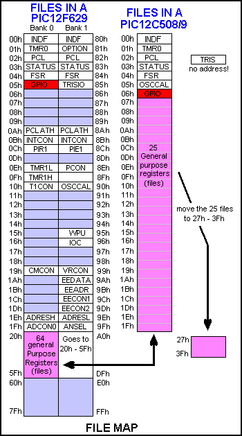
The in/out port (file 05h for PIC12F629) is shown in RED in the following map. It is called GPIO:
Voltage on an Input line
Most input lines are
classified as TTL and the voltage must be above 2v (for 5v rail) for the chip to
detect a HIGH. GP2 is Schmitt Trigger input a it TMR0 clock input. This
line requires 2.5v to detect a HIGH and 1.75v to detect a LOW. The TTL input
have a very small gap between HIGH and LOW and to make sure the input line
detects correctly, the input voltage must be much higher or much lower than the
detection-point.
4. Reading the Input Port
To read the individual
pins of the input port of a PIC12F629, use one of the following instructions.
(GPIO,3 (GP3) (pin 4) is an INPUT-ONLY pin and this pin is the first to
use.
If the input pin is normally low and goes HIGH when a signal is sent to the
micro, use one of the following:
btfsc 05h,0 (This the same as: btfsc
GPIO,0)
btfsc 05h,1
btfsc 05h,2
btfsc 05h,3 - this is pin 4 - GPIO,3 - use
first in your program
btfsc 05h,4
btfsc 05h,5
The next instruction will be:
goto task1 - input has been detected
It may be difficult to read the same input bit
further down a program.
This is solved by setting and clearing the bit, thus:
bsf
status, rp0 ;Bank 1
bcf
TRISIO,0
nop
bsf
TRISIO,0
bcf
status, rp0 ;bank 0
5. The
General Purpose Files - called GPR's (General Purpose Registers)
The General Purpose
Files are the files you use in your program for sub-routines such as delays,
comparison, incrementing, decrementing, etc. A program can start by loading a
value into GPIO and outputting it to the outside world (such as a LED). A value
(called a literal) is loaded into a file (a General Purpose File) and
decremented until it is zero. This allows the
LED to be viewed.
In the diagram above, you can see the 25 General Purpose Files in a PIC12C508/9
do not match up with the 64 files in a PIC12F629.
This means any program written for a '508 will not work in a PIC12F629.
The solution is to add 20h to the files that have been used in a '508 program to
move them so they align with the PIC12F629 files.
The following table shows the result:
| Old '508 file: |
for '629 |
|
| 07h | ð | 27h |
| 08h | ð | 28h |
| 09h | ð | 29h |
| 0Ah | ð | 2Ah |
| 0Bh | ð | 2Bh |
| 0Ch | ð | 2Ch |
| 0Dh | ð | 2Dh |
| 0Eh | ð | 2Eh |
| 0Fh | ð | 2Fh |
| 10h | ð | 30h |
| 11h | ð | 31h |
| 12h | ð | 32h |
| 13h | ð | 33h |
| 14h | ð | 34h |
| 15h | ð | 35h |
| 16h | ð | 36h |
| 17h | ð | 37h |
| 18h | ð | 38h |
| 19h | ð | 39h |
| 1Ah | ð | 3Ah |
| 1Bh | ð | 3Bh |
| 1Ch | ð | 3Ch |
| 1Dh | ð | 3Dh |
| 1Eh | ð | 3Eh |
| 1Fh | ð | 3Fh |
6.
Incrementing a File
When incrementing a file
such as:
incf 2Ah,1
The result is placed in the file and the working register "W" is not affected.
With the instruction:
incf 2Ah,0
only the working register "W" contains the result. In other words,
the file is
NOT INCREMENTED!!!
With the instruction:
incf 2Ah
the assembler assumes ",1" and increments the file. But it is best to
always include the directive.
In the above, W=0 and f=1 where W is the working register and f is the file
being incremented.
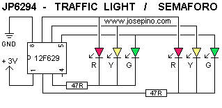
7. Current of an Output Line
The maximum current of an output line is 25mA. In the
following diagram, no current-limiting resistors have been included and the
current through the red LED will be more than 25mA as the voltage across the LED
is 1.7v and theoretically the current will be as high as the battery can
deliver. The chip will provide some current-limiting but the flow will be higher
than 25mA and the chip may be damaged. A PIC12F629 will deliver about 33mA if a
current-limiting resistor is not included, or is too-low in value.
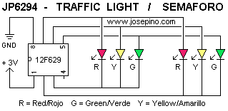
Two 47R resistors are needed as shown in the schematic below:
8. Driving a LOAD
The output current of each line of a microcontroller is very
small. It is only 25mA. The only two items that can be driven directly from an
output are a LED and a mini piezo diaphragm.
The following diagram shows how these items can be connected (interfaced).
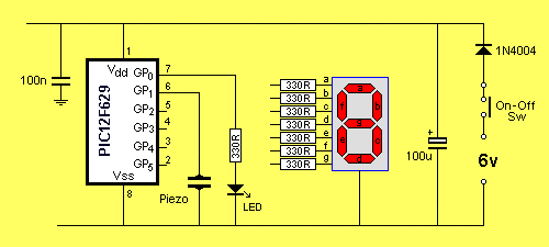
For a current greater than 25mA, a transistor will be needed. A transistor will
be able to deliver about 500mA to 1Amp. This is assuming the transistor has a
gain of 20 - 40 and this about the capability of a transistor - called a
small-signal transistor.
For larger currents, a MOSFET will be needed. These devices will deliver 20 amps
or more to a load.
There are two ways to describe the requirement of "driving a load."
You can say you want to "drive the transistor as an amplifier" or "drive the
transistor as a switch."
When a transistor is used in an analogue situation, there is a big difference
between these two statements.
In an audio amplifier, when the transistor is amplifying the signal, the output
is a faithful reproduction of the input, but with a larger amplitude. Or the
shape of the signal will be identical but with a larger current capability.
But if the transistor in an audio amplifier is driven as a switch, the output
will rise very high as soon as the input waveform starts to rise. In most audio
cases this will create distortion.
But with a microcontroller we are dealing with a digital circuit and the output
is either 0v or rail volts (5v).
Any transistor connected to the microcontroller can only have two states. When
the output is zero, the transistor is turned off. This is called CUTOFF. When
the output is high, the transistor is turned ON fully. This is called
SATURATION.
These two states are called SWITCHING STATES. When a transistor is in either of
these two states, it dissipates the least amount of heat. When a transistor is
CUTOFF it is obvious that the heat dissipation is low as it is zero.
When a transistor is SATURATED, it has the lowest voltage across it and although
the current flow is the highest, the heat dissipated is the lowest as the heat
loss is multiplication of current and voltage.
Suppose we want to drive a wailing siren from a microcontroller. If the
microcontroller delivers the varying tone to the speaker, we say the transistor
is acting as an amplifier. It is acting as a DIGITAL AMPLIFIER. It is being
switched ON and OFF at different rates and the result is a wailing sound.
When we refer to the transistor as a SWITCH, we often require it to turn on a
device for a long period of time - such as a relay or LED.
8a. Driving a LOAD - circuit TRICK:
You can increase the current to a pair of Infra-red LEDs from
25mA to 39mA by adding the 120R resistor.
To do this there are a number of calculations to remember:
The voltage across an IR LED is about 1.5v to 1.7v and an IR LED can be driven
at a higher current than an ordinary LED.
Some IR LEDs accept 100mA or more for a very short pulsed duration and this
arrangement will produce 39mA.
When the drive-line is HIGH, it delivers 25mA and the 120R delivers 13mA, making
a total of 39mA.
When the drive-line is LOW, it sinks the current through the 68R and 120R (in
series) and this is 25mA. The voltage across the two IR LEDs is 1.8v and this is
below the "turn-ON" voltage for the two LEDs.
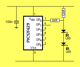
Increasing the output current
9. GP3 - pin 4 Driving a LOAD
THE PIC12F629 - some preliminary
points:
GP3 is an INPUT Only and cannot be used to drive a load.
The only drive-lines for PIC12f series are:
GP 0 - pin 7
GP 1 - pin 6
GP 2 - pin 5
GP 4 - pin 3
GP 5 - pin 2
10. 100n across the micro
Don't forget the 100n across the power rails. Place it near the micro. It
stops the micro starting-up half-way through the program! Without the capacitor,
the micro can start anywhere down the program and create all sorts of unusual
effects.
11. The Hysteresis
The input lines of a PIC chip need about 5v to detect a HIGH
and about 0v to detect a LOW.
But when the voltage is about 2.5v, it will register a HIGH at about 2.01v and a
low at about 1.99v.
This means the gap between a HIGH and LOW is very small and this gap is called
the HYSTERESIS.
SOME APPLICATIONS:
Although the PIC12F629 is the simplest device
in the PIC range, it can can carry out operations such as monitoring and
controlling:
![]() Battery
Monitoring and Voltage Detection
Battery
Monitoring and Voltage Detection
![]() Watchdog
Timing
Watchdog
Timing
![]() Circuit
Resetting
Circuit
Resetting
![]() Voltage
Detecting
Voltage
Detecting
There are many specially-designed chips for these applications, but they
must be purchased in large quantities. To keep your inventory down, you can use
a PIC chip with a few external components to perform the operation. All you have
to do is design the circuit (the detection section) and program the chip.
READING A PIC CHIP
If you have a
PIC12C508/9 chip and want to get the program and convert it to suit a
PIC12F629, you will need to fit it into the socket of our
Multi Chip Programmer
and read it via ICProg.
To do this you will need to pick PIC12C508 from the list of microprocessors from
the "drop down" menu. You will also need disasm.dll
or the Disassembler link above.
For disasm.dll, use the "lightening" symbol to import the code from the chip. It will appear in
the frame on the screen. Use the "A" button (next to the "H" button) to see the
disassembled program.
You can then copy and save the program in Notepad. Only chips that are not
Code Protected, can be read. We only have some information on reading
chips that are Code Protected:
Cracking a PIC Chip
If you have the .hex file, you can get the assembly file via
disasm.zip as
explained above.
Once you have the assembly file, you can change the files as shown above.
SOME PROGRAMMING TRICKS:
The author has found problems with some
instructions.
The PIC12F629 does not like setting a bit on the in/out port and then setting or
clearing another bit in the next instruction.
The problem instructions are something like this:
bsf 05,2
bsf 05,4
The micro does not set the second bit when it is executing the program. The
answer is to work out the value in file 05 before the two instructions, add the
value of the bits and place the value in the in/out port via the following two instructions:
movlw xxh
movwf 05h
Alternatively, a meaningless instruction can be inserted between the two "bsf"
instructions. This MAY work but is not as guaranteed as the method above.
bsf 05,2
nop
bsf 05,4
Each new program or modification MUST be saved with a new name as either MPASM
or IC_Prog will not detect the changes and you will get the old program burnt
into the chip and wonder why the changes did not fix the problem!
USING A SIMULATOR AND
DEBUGGER
To help developers get a program to work
successfully, a number of programming tools have been created. Two of these are
a SIMULATOR and a DE-BUGGER. These are software programs and a simulator runs
your program and lets you know if it will work. It seems to be the answer to a
dream. But a simulator has many limitations. It assumes any hardware devices
connected to the program are "ideal devices."
For example, it will assume a switch has no "contact bounce" and is pressed and
released very quickly. This does not happen in real life, so your program must
be re-tested in actuality.
Also, any output to LEDs etc assume the items are connected around the correct
way. You will still have to test the actual circuit and make sure the current is
within the limits of the micro.
A de-bugger is also another piece of software that tries to locate a fault in
your code.
It has a "single step mode" in which it shows the contents of each register
after an operation.
Sometimes these program will assist but let me assure you that they can also
lead you "down the garden path" and in the wrong direction.
I have used them and concluded that they create more frustration than
assistance.
The best method is to start with a small number of instructions and make sure
the program works. Add a few more instructions and re-test the program. Re-name
the file each time you add instructions and slowly build up the program. This is
the best way to avoid frustration.
We have provided explanations and helpful advice in our
Library of routines:
A-E
E-P
P-Z
and provided a number of programs for you to analyse and use. The main thing is
not to use an instruction unless you know exactly what it does. Do not try any
"clever" programming, with exotic instructions as the result can be completely
different to what you expect.
The first thing to do create a subroutine called a delay. Call it
"_200mS" for 200milliseconds delay.
_200mS movlw 0C8h
; equal to 200
movwf fileB
AA decfsz
fileA,1
goto AA
decfsz fileB,1
goto AA
retlw 00
Create a routine to turn a LED "on" and "off" using the delay.
such as:
On_Off bsf gpio,0
; put a LED on pin 7 with a 470R resistor.
call _200mS
bcf gpio,0
call _200mS
goto On_Off
If you want to see if the micro has advanced down a program to a particular
location, put:
goto On_Off and the LED will blink.
SOME CIRCUIT TRICKS:
The author has found the PIC12F629 chip must
be fitted to a circuit when the voltage on the rail is ZERO. If a voltage is
present, some of the files in the chip will get corrupted and the program will
not run correctly. For example, some of the outputs will not go HIGH when
required. The remedy is to turn off the project and wait for the electrolytics
to discharge. You can also remove and replace the chip if you find it is
performing incorrectly.
The addition of a 10k resistor across the power rails will discharge the
electrolytics to zero and help solve this problem.
Also, the addition of a 100n (very close to the chip rails)
will provide stability for the chip and allow the internal
oscillator to work correctly and prevent outside spikes from upsetting the chip.
The PIC12F629 is an 8 pin
chip that can be re-programmed up to 1,000 times.
It is an up-grade of the PIC12C508 and '509 as it can be re-programmed.
(The PIC12F629 does not have analogue inputs - the PIC12F675 has 4 analogue
inputs.)
For more details on PIC chips, see our
Chip Data Ebook.
Here is a list of the chips we suggest for the beginner to microcontroller
programming.
Start with the 8-pin 12F629 if you have only 1 to 5 items to "drive"
(GP3 is input only). Or use the PIC16F628A if you want to
drive up to 15 items (RA5 is input only).
| Device | No of pins |
Type | Code Space |
I/O Pins |
ADC Pins |
ADC |
We use these: |
||
| PIC12C508(A) | 8 | OTP | 512 | 6 | Data | ||||
| PIC12C509(A) | 8 | OTP | 1024 | 6 | |||||
| PIC12F629 | 8 | Flash | 1024 | 6 | Data | ^ | Smallest chip 1st choice |
||
| PIC12F675 | 8 | Flash | 1024 | 6 | 4 | 10-bit | Data | ||
| PIC16F84(A) | 18 | Flash | 1024 | 13 | Data | ^ | Lots of projects for this chip |
||
| PIC16F628A | 18 | Flash | 2048 | 16 | Data | ^ | 2nd choice |
The smallest, simplest, and latest 8-pin microcontroller chip in the PIC series is
the PIC12F629. It has 8 pins, will accept over 1022 lines of code and can be
re-programmed over 1,000 times. It has 6 in/out lines (GP3 is input only) and
will deliver about 25mA on each output.
Programs and projects written for the PIC12C508 and '509 can be converted
to
PIC12F629 by using our
blank12F629.asm
template.
The only items that have to be converted are:
(a) The config values. ( __config) The configuration values
that turn things on or off, such as the watchdog timer, internal oscillator,
plus others, to suit the PIC12F629.
(b) The GPIO values.
GPIO for PIC12C508A is location 06h
GPIO for PIC12F629 is location 05h
To convert a PIC12C508 assembly program to 12F629, the in/out instructions (such
as 06,0 06,1 etc) are converted to GPIO,0 GPIO,1 etc.
In one of our articles we explained how to produce a program in a
PIC16F84A and when the project is working perfectly, the program can be
burnt into a
PIC12C508A. This was necessary as the PIC12C508A was One-Time
Programmable device. The
GPIO's for PIC12C508A are in location 06h.
This is
Port B for a PIC16F84A or 06h. (Port A for a PIC16F84A is 05h).
If you use the PIC12F629, you do not have to create your program in a PIC16F84A
as the PIC12F629 can be programmed up to 1,000 times.
(c) The TRISIO for a PIC12F629 is address 85h in bank 1. Use the instruction
TRISIO when programming a PIC12F629. For a PIC12C508, the instruction is
TRIS. It has no address.
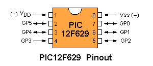
IDENTIFYING THE PINS
The pinout of the
PIC12F629 is the same as the PIC12C508A and all projects using a '508A
can be converted to PIC12F629 by fitting a PIC12F629 and turning the project on.
All you have to do is burn the '508A program into the PIC12F629 before fitting
it.
Only a few lines of the program and a few instructions are different for the
PIC12F629 - these are the setting-up instructions and the location of the GPIO
file. The differences have been discussed above.
Many of the pins have a dual function and the first thing to do is decide on the
function of each pin. In most cases you will want to use the oscillator inside
the chip and this will allow you to use all the 6 in/out lines.
The functions for the chip will be simplified to:
The setting-up of the pins, plus the other functions of the chip, is done via an instruction called "__CONFIG." - Note the double
under-bar: __
This instruction also determines a number of other things for the chip, such as
code protection, and watchdog timer.
During experimenting, turn Code Protection OFF and Watchdog Timer OFF.
This will allow you to read a chip. Before marketing the final design, the code
protection is turned on and the chip is "protected." If the watchdog timer is turned off, you
will not have to include instructions in your program to keep resetting the
timer. This is a complex thing to do and will be discussed later. Keep things
simple for the moment.
MCLR
Pin 4 can be configured as an "Input line" (GP3) or "Master Clear."
To configure Pin 4 as MCLR
(also written as /MCLR or /MCLRE ) the configuration bit setting is: _MCLRE_ON
When this pin is configured as /MCLRE, the pin resets the chip when it is taken
LOW.
To configure Pin 4 as GP3, the configuration bit setting is: _MCLRE_OFF
This instruction tells the PIC to use its internal MCLR circuitry (to keep /MCLRE
high), and leaves
pin 4 free as an Input line. Note: MCLR pin (GP3) is INPUT ONLY.
OSCILLATOR CALIBRATION VALUE
Calibration of the oscillator is only necessary when
you need precise timing, as for serial communication. In most cases you will not
have to worry about this.
The oscillation calibration value can be changed from the
value supplied in the chip by adding the following instructions to the end of
your program, (BEFORE the "end" instruction of the program).
|
;**************************************************************** ;* OSCCAL calibration value * ;**************************************************************** org 0x3ff retlw 0x20 END |
During the programming of the
chip, the above instruction will cause the burner to go to location 3FF and
insert the value 20h as well as the instruction "return with the value 20h in
W."
To create the maximum frequency, use: 3fh
Centre frequency = 20h
Minimum frequency = 00h
During the running of the program (when the chip is in the project), this value
is put into the OSCCAL location, to adjust the frequency of the internal
oscillator.
To get the micro to do this, the following instructions are added to your
program:
|
;**************************************************************** ;* Calibrating the internal oscillator * ;**************************************************************** bsf status,rp0 ;bank 1 call 3ffh ;get the calibration value movwf OSCCAL ;calibrate bcf status,rp0 ;bank 0 |
The location of the oscillator calibration register is 90h. This is in Bank 1
and is identified in your program by writing: "OSCCAL"
It is a 6-bit register, with values from 00h to 3fh.
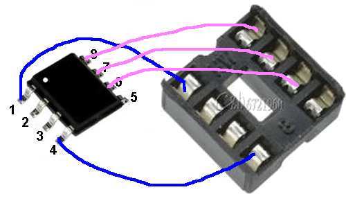
SURFACE MOUNT PIC12F629
The surface
mount PIC12F629 is just as easy to use as the through-hole version and makes a
project very small and compact.
You can reprogram the chip after you have soldered it to a project by using the
PIC Burner Board from Talking Electronics and PICkit2 programmer and buying an
8-pin surface mount holder for the chip and soldering it to a socket as shown
below. The second images shows the surface-mount holder with the chip. Remove
the divider in the centre of the holder so you can use tweezers to fit the chip.
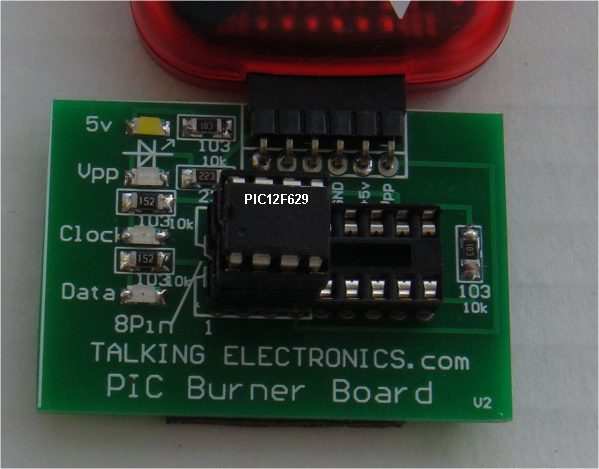
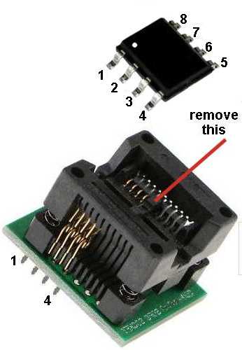
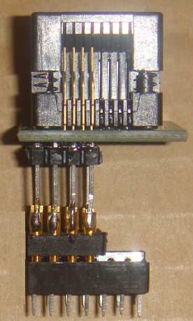
Then fit the 14 pin IC socket to the burner board and the socket gives
additional stability.
If the chip is driving LEDs, the output pins of the chip can be driven high
enough so the chip can be re-programmed after it has been fitted to a project.
To re-program the chip you will need an 8-pin socket and 5 wires. These wires
can easily be soldered to the pins when the chip is in the project and quickly
desoldered when the new program is working.
I have not damaged or wasted a chip and re-programmed then with a new program in
an old project. I have also soldered and de-soldered and resoldered a chip and
it worked perfectly.
1-8-2020