|
The |
STARTING
In this article you are going to
learn how to really design a transistor amplifier and forget everything
you have been shown and told and learnt.
All the YouTube Videos, University Video course and everything you have
seen is totally irrelevant, distracting, inaccurate and worthless.
They all treat you live a cave dweller without the knowledge of
electricity whereas the fact is different. Everything you need is
available as examples on the web and all you have to do is copy a
circuit diagram and try it. You don't nead any mathematics and
very little understanding.
All you need is a set of components and a simple multimeter and be
prepared to experiment.
That's how I leant. 3 years of an electronics course taught me NOTHING
and when I entered an electronics repair shop, I suddenly realised I had
been taught nothing. All the lectures were "smoke and mirrors" and
"befuddlement" and "complication." I didn't have a clue how to fix
anything. But I am very smart and there is nothing faster than
"self teaching."
Simple transistor circuits are NOT designed like you see in any text
book, video or University lecture.
They are designed completely differently but none of the lecturers have
designed a circuit in their life and and have no idea what they are
teaching.
You are going to learn that you cannot design a circuit (using
mathematical equations) to produce
mid-rail biasing as the actual set-point depends on the gain of the
transistor and the biasing values are very very critical. Any instructor
that says he can set the value does not have a clue about circuits. I
have not found a single YouTube video that teaches the correct approach
or anything that you can apply to real-life designing, so you need
to start with a completely fresh approach and realise everything is
actually done completely differently to what you have been taught.
We are going to start with the SELF BIASED TRANSISTOR AMPLIFIER.
Commonly called the COMMON EMITTER AMPLIFIER. (The other circuit is
called the H-Bridge configuration)
Here is the circuit. It uses real values because that is the only way to
learn. And it does produce a fairly accurate mid-rail biasing.
Whistle into the microphone and the circuit will produce a 4 volt
waveform. You can change the LOAD resistor from 22k to 47k or down to
10k and the output will alter very little. You can change the base bias
resistor from 1M to 2M with very little change in the output waveform.
Build the circuit and you will get a shock. It produces a small
output signal. And the values of base-bias can be critical.
Unless the lower base bias resistor is between 16k and 19k the circuit
may not produce an output.
The BC 338 emitter-follower transistor will have a gain of say 100. This means it will
amplify the resistance of speaker 100 times to get an impedance of 800
ohms on the base of the transistor.
Just because the output impedance is 22k and the driver stage is 80,000
ohms, does not mean there is any miss-match. You have to realise
the impedance will be so high that it does not reduce the amplitude of
the signal of the first stage.
THE THIRD
ARRANGEMENT
This has one major drawback because the collector of the upper
transistor (within the Darlington transistor) is not connected to the supply rail but to the speaker.
This makes an enormous difference to the way the transistor works. I am
not going into the technical aspects except to say the collector-emitter
voltage is never less than about 1.5v to 2.5v due to the way the
Darlington transistor operates. The end result is about 4v across the
speaker and this is no better than the previous arrangement.
THE FOURTH
ARRANGEMENT
The BC547 and BC338 transistors are connected "on top" of each other and
they form a single transistor with a very high amplification factor.
Now you can see the uselessness and stupidity of all the common-emitter
discussions in text books and YouTube demonstrations.
ooooooooooooo0000000000000000000oooooooooooooooooooo
It
will be years before you can do the same, but we can start with the
principles of how a transistor REALLY WORKS.
Simply replace the transistor with a POTENTIOMETER. Look at how we have
changed the transistor into a "pot."
You now have two resistors in series.
The VOLTAGE DIVIDER is simply two resistor in series. When the lower
resistor is a VARIABLE RESISTOR the voltage at the join will INCREASE or
DECREASE.
HOW DOES THE CIRCUIT WORK?
Now, T
We will take the Self Biased Transistor Amplifier and see how it works.
All you have to do is work out what voltage will appear at the join and
you will find it only a very small voltage and that's how the circuit
has the potential to produce a very good output waveform. And if I go
into further investigation I will get a very accurate outcome without
any mathematics or equations or frustration.
When designing and diagnosing the Self Biased Stage (with electret
microphone), Fig 8 converts all the active components into variable
resistors as shown by the symbol that will be new to you..
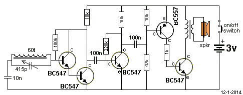
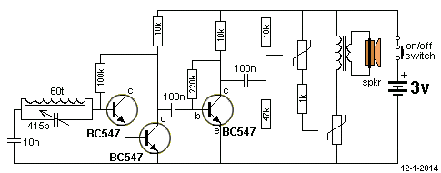
Now we come to a 5 Transistor Radio.
The two transistors are replaced with variable resistors and the top
variable resistor will be reduced in resistance by the signal through
the 100n capacitor.
We have covered all the stages except the third transistor.
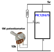
ANOTHER EXAMPLE
That's why you have to see the IR transistor as a variable resistor ,, ,
as shown in the following diagram.
When the potentiometer shaft is rotated to full resistance, a
voltage-divider is set-up between the pot and 10k load resistor. . . . .
. . 10k is in series with 1Meg ohms. You need to understand voltage
dividers and very little voltage will be "dropped" across the 10k.
If the supply is 5v, pin5 of the micro will see 4.95v
The solution is to increase the LOAD resistor to 100k. The voltage
at the join of the resistors becomes 100k:10k and to keep things
simple, the voltage across the 100k is 4.5v and the input of the
microcontroller sees 0.5v. This is low enough for the micro to register a
LOW.
This is the IR transistor and 100k LOAD:
Here's the way to look at the circuit. The IR transistor can only pass a
certain amount of current.
This discussion has shown how I "see" circuits working in my mind.
Another 100 Transistor Circuits can be found
HERE.
Go to
Talking Electronics
website
21/1/2024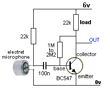
Fig1: The
self-biased Transistor Amplifier
These changes hardly affect the performance of the circuit because the
transistor is creating its own OPERATING POINT. You are not forcing any
conditions on the base (the H-Bridge has a tighter hold on the biasing
of the transistor).
To create this circuit you simply use 22k for the load resistor for 3v
or 6v supply (47k for 9v to 12v supply) and start with 1M for the
base-bias resistor. Increase the value until you get half-rail-voltage
on the collector. You must use only a digital voltmeter for measuring
the voltage.
Now we come to the COMMON EMITTER CIRCUIT described on the web in so many
YouTube videos, as the H-Bridge design: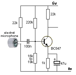
Fig2: The H-Bridge Transistor Amplifier
330k and 47k work best
We used 330k and 47k to produce a 4v output and when the 47k was reduced
to 39k, the output dropped to less than 2v. The biasing components
are critical and there is no way to design the circuit
mathematically. You need to experiment with the values to see the
effect.
This is something that not one of the videos tell you. None of the
instructors have built the circuit and none of them know what they
are talking about.
By changing the biasing components you are allowing the transistor to set its own conditions of BIASING.
The base biasing resistors set the condition called QUIESCENT or REST condition. But you do not
know what biasing values to use.
150k and 47k did not work, 330k and 47k worked perfectly. What
mathematical formula could you use to achieve the best result????
You cannot use any equations. The values of resistor will vary
enormously because the gain of the transistor can be from 150 to 450.
The only way is to build the circuit and experiment.
CONCLUSION
Both the above circuits were built in December 2023.
Using 330k and 47k for the second circuit, the electret microphone
delivered a 20mV output with 22k load resistor. This signal was not
appreciably attenuated when connected to the two transistor amplifiers
and the output at the collect was about 2v p-p. (There was a small
attenuation but I could not measure it.)
We concluded that both circuits produced the same results.
The electret microphone detects a pin dropped on the floor and you can
listen to voices in the next room with a clarity that is better than normal hearing.
The two circuit have not increased the current-capability of the signal
as the impedance of the electret microphone is 22k and the impedance of
the amplifying is 22k (as determined by the value of the collector load
resistor).
However the amplitude of the signal has increased from 20mV to 2,000mV
and it is an increase of 100 times. So the stage has achieved
something.
A stage can increase just the amplitude, or just the current, or both.
And if the answer is about 100 we have been successful.
We now have to connect the output of this stage to a second stage.
The first amplifying stage is called a PRE-AMPLIFIER and the second
amplifying stage is called a SMALL SIGNAL AMPLIFYING STAGE as it must be designed to have a high impedance input, so it does not load the first
stage.
So far, we have not increased the "strength" of the signal. It is just
as weak as the signal emerging from the electret microphone. All we have
done is is increase its amplitude.
You just cannot connect it to "anything" (such as an earpiece
or speaker) because if you reduce the
amplitude, you will have lost some of the benefit of the first stage.
And it is too weak to drive anything such as an earphone or speaker. .
But, unfortunately, the second stage will require some of the energy
(signal) from the first stage, for its operation.
Our skill is to lose
as little of the amplitude as possible. More accurately, we want to lose
as little ENERGY as possible.
In other words, the input of the second stage must have a high input
impedance.
If we connect the stage to an input impedance of 22k, the signal will be
attenuated by 50%. This is because the 22k LOAD resistor will be in
series with 22k of the second stage and it will form a voltage divider
of 50%.
If the impedance of the second stage is 10k, the signal will be reduced
to 30% or less.
To have the smallest attenuation we need the input impedance to be 100k or
higher.
Let's say we want to drive an 8R speaker.
We will look at 4 different amplifying stages and see what results we
obtain.
The first is called
an EMITTER FOLLOWER STAGE.
It increases the current by 100 times (or more.)
The following diagram shows this arrangement: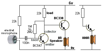
Fig3: Connecting an
EMITTER FOLLOWER stage
You don't need any mathematics, just an understanding of how the circuit
works.
The 22k collector LOAD resistor and the 800 ohms impedance of the
speaker will form a voltage divider and the voltage across the 800 ohms
will be less than 5% of rail voltage.
This is almost useless for a speaker and shows the stage cannot drive a
speaker.
The first secret you have learnt is the emitter follower stage multiplies the impedance
of the speaker by a value equal to the gain of the transistor. The gain
may be 150, 250 or slightly more.
Secondly, the first transistor does not deliver any energy to the
emitter-follower stage. The 22k LOAD resistor delivers the energy. The
first transistor simply turns OFF and the 22k delivers the energy.
The transistor turns ON to produce the lower portion of the wave.
But it is the 22k that delivers the rising portion of the signal.
That's why a single emitter-follower stage will not work.
If we add another emitter-follower transistor we will increase the
impedance by 100 times and now the ratio of the 22k to the impedance of the output
stage will be 80,000 ohms and it will not reduce the amplitude of the
signal produced by the 22k. That's because the voltage division
has a ratio of 22,000:80,000 or about 25%. In reality the ratio will be
a lot more beneficial and the the two transistors will deliver almost
full amplitude from the first circuit.
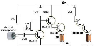
Fig4: Connecting two
EMITTER FOLLOWER stages
However the maximum amplitude will be reduced by about 1.5v due to the
two base-emitter drops and the output will be about 4v. This is always
the case
with emitter-follower stages using two transistors.
The current delivered by the circuit will be: 4v/8R = 0.5A
and this will only occur when the transistor is not conducting and the
22k is pulling the two transistors HIGH.
You can use a single Darlington transistor in the output to get the
same results.
The third way to
drive an 8R speaker is to
use a Darlington transistor in place of the two
individual transistors as an EMITTER-FOLLOWER.
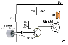
Fig5: Connecting a
Darlington transistor
Here's
another way to see the circuit: If the Darlington transistor has a gain
of 80,000 it will divide the effectiveness of the 22k by 80,000.
If the gain was 22,000 the 22k divided by 22,000 would result in one
ohm. But if the Darlington is 80,000 the result is 1/4 ohm.
In other words the Darlington gets converted to a 1/4 ohm resistor with
a characteristic voltage across the collector-terminals of about 1.5v to
2.5v This is how you diagnose circuits quickly and easily.
The fourth way to drive an 8R speaker is to place the BC547 and BC338 in
a SUPER-ALPHA arrangement.
This is shown in the following diagram: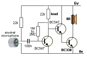
Fig6: Connecting a
SUPER-ALPHA pair.
This time we cannot say the impedance is 80,000 ohms but we can say the
pair will amplify the current provided by the 22k by a factor of about
100 x 100 = 10,000 times. We don't know how much current will be
supplied by the 22k but suppose it has 1v across it, the current will be
1/22,000 amp. If we multiply this by 100 x 100 we get 100/22 amp
and this is obviously more than the battery will deliver, so the circuit
will certainly drive the speaker.
There will be a very small voltage across the collector-emitter junction
of the BC338.
By re-positioning the two transistors we improve the signal from 4v to
nearly 6v.
This is the best arrangement and we have shown the disadvantage of a Darlington transistor.
These 4
arrangements are called IMPEDANCE MATCHING. Impedance Matching is
the art of using the available current and voltage from a stage and not
reduce it. In other words the stage you are adding has to provide
the energy to drive the LOAD. If the stage you are adding does not do
this, the circuit will take energy from the first stage and reduce the
amplitude of the signal.
That is the basics of Impedance matching. Sometimes, the amplitude of
the signal will be reduced but the circuit will adjust and an accurate
waveform will appear in the LOAD. So, there is no clearly defined way to
connect stages and the only success is listening to the result. You can
hear much more of the quality than any signal on an oscilloscope.
Some output stages need a large voltage swing and some don't. Some
only need 50mV. But they all require a certain amount of current
and each transistor in the output stage amplifies this current 100 to
300 times.
How do you work out if
arrangement #4 will work?
Maximum voltage across
the 22k is: 6v minus 0.7v minus 0.7v =
4.6v
The max current that will flow in the 22k resistor will be 4.6 /
22,000 amp
The first transistor in the driver stage will amplify this current by
about 250 to 300 times.
And the second transistor in the driver stage will amplify about 100
times.
This means the circuit is capable of delivering: 4.6 / 22,000 x
300 x 100 = 4.6 x 3 x 10 / 22 =
46 x 3 / 22 = 2 x 3 = 6 amps.
This is obviously much more than required by the speaker (5.8 / 8
= less than 1 amp) and so the driver stage will be suitable.
You cannot design a circuit without knowing the current capability and
amplitude of the input signal and the characteristics of the stage you
will be connecting to the output. These two affect the operation
of the stage enormously.
A REVOLUTIONARY UNDERSTANDING
Now we come to the next piece of revolutionary understanding.
I can see the operation of every circuit "in my mind."
Forget all the RUBBISH you have seen and learnt and read in text books
and on the web.
None of it will help you understand and design and "see" how a circuit
works.
I bet you have never been told a transistor does not deliver energy to
the following stage. It is the LOAD resistor that delivers the energy. I
call it: "failure by omission." None of the writers have ever designed
or repaired a project. They simply repeat what they have read and been
told.
There is an old saying. If you can: "Do."
If you can't. "Teach."
A transistor is just a VARIABLE RESISTOR - a POTENTIOMETER
Here is the circuit of a REAL TRANSISTOR: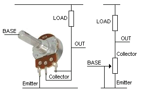
Fig3: The Transistor is
simply an adjustable resistor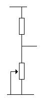
Fig4: Two resistors
Two RESISTORS IN SERIES is the basis of a VOLTAGE DIVIDER. And that is
what each section of a circuit becomes. It becomes a VOLTAGE DIVIDER.
Now I can tell you the most outstanding comment you will ever hear. The
potentiometer cannot produce any amplification. No voltage amplification
and no current amplification. And a transistor cannot produce any
voltage or current amplification either. You have been
fooled.
It is the LOAD RESISTOR that provide and produces and assists and is
essential in creating these features.
And only when you realise the LOAD RESISTOR creates all the magic, will
you understand how a circuit REALLY WORKS.
Just because the transistor increases the base current by 100 or 200,
does not make the circuit "move" or "work."
The whole circuit works on the VOLTAGE DIVIDER principle.
Fig5: The VOLTAGE DIVIDER
When the resistance of the variable resistor increases, the voltage at
the join increases.
That means: When the resistance of the transistor increases, the
output voltage increases.
But you must understand this as: The top resistor PULLS the
voltage high. The transistor merely ALLOWS the LOAD to pull
the output voltage HIGH.
Now, depending on the value of the LOAD RESISTOR, and the ability of the
transistor to pull the output voltage LOW, the amplitude of the output
is created. The transistor PULLS the output LOW and the LOAD RESISTOR
pulls the output voltage HIGH.
But the LOAD RESISTOR can only pull the output voltage HIGH when the
transistor stops pulling it LOW.
If the transistor can "pull-down" very strongly, the LOAD resistor can
be a small value of resistance and this means the current in the circuit
will he high.
If the LOAD RESISTOR is a high value of resistance, the transistor
will find it very easy to pull the output down to a low value. And this
means only a small current will be present.
If the LOAD RESISTOR is a very LOW value of resistance, the transistor
will not be able to pull the output down AT ALL (if the transistor is
weak).
The input lead of the transistor is the BASE and it needs CURRENT.
Current has MUSCLE and it will turn the shaft of the variable resistor
to produce a LOW VALUE of resistance.
In actual fact, the transistor increases the "strength" of the input
current 100 times (or more) to turn the potentiometer shaft.
THE NEXT POINT
If the value of resistance of the LOAD
RESISTOR is HIGH, only a very small current will flow in the voltage
divider and only a very small current will be available on the OUTPUT.
If the values of resistance of the LOAD RESISTOR is SMALL, a HIGH
current will flow in the voltage divider and a HIGH current will be
available on the OUTPUT.
This means the output current will depend on the value of resistance of
the LOAD RESISTOR. As long as the transistor can pull the output voltage
down to a very small value, the value of current depends only on the
LOAD RESISTOR.
You also have to understand the output voltage
depends ONLY on the LOAD RESISTOR, (when the
transistor is able to pull the output voltage LOW).
So, all we have to do make sure the transistor can pull the output
voltage LOW and the amplitude and output current capability will depend
on the value of the LOAD RESISTOR.
Here's the next amazing thing you will learn:
Fig6: The
Self Biased Transistor Amplifier
When the stage is sitting with no audio input, nothing will be
processed.
But a tap on the microphone will reduce is resistance (impedance) and
the voltage to the 100n coupling capacitor will fluctuate up and down
and when the cycle produces a rising voltage, the first 22k LOAD RESISTOR will do the "pulling up."
Now, what we say is: 22k is entering the transistor
amplifier and the transistor reduces this value by 100 to 200 - as this
the gain of the transistor - and it becomes 22,000/100 = 220 ohms.
That's right!! The transistor deals with the input and turns
it into a 220 ohm resistor, exactly like fig7: 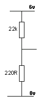
Fig7: 22k:220R voltage divider
I will get a much closer result than any mathematician because I KNOW
WHAT I AM DOING.
Technically we have not achieved much in this circuit because the first
load resistor is the same value as the second. But we have created an
increase in amplitude. But the main aim for each stage is to
create an increase in current. Otherwise the stage is called an
INTERFACE STAGE to connect two items with different impedances.
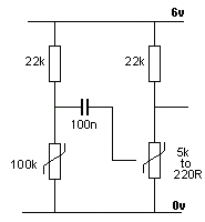
Fig8:
That's all I see. The electret microphone can pull the 22k
down a small amount and then the capability of the 22k will pass to the
transistor via the 100n and get converted to 220R and this value,
combined with 22k LOAD resistor will produce a HIGH and LOW output equal
to about the 6v supply.
We have to convert a 5mV signal with 1microamp capability into a 3v
signal with about 50milliamp capability.
The first stage consists of 2 transistors "on top of each other."
This is simply a single transistor with a very high input resistance
(impedance), so it does not put a load on the tuned circuit.
Basically it will multiply the 1 microamp by a factor of about 100 and
the other transistor will increase this 100 times. So 1 microamp
becomes 100 microamps x 100 = 10,000 microamps which is 10
milliamps. But lets reduce this to 1 milliamp. One milliamp
flowing through 10k, resistor will produce a voltage drop of 10v. But we
only have 3v, so the output will be quite sufficient for the radio.
So, now we have theoretically plenty of current and a high voltage
swing.
The next stage simply increases the swing slightly and brings the
current up to 1mA.
The final stage consists of two directly-coupled transistors.
This is the job or function result they must perform or carry-out.
The signal into this section has an impedance of about 10k and a current
of less than 0.3mA and maybe a voltage swing of 2v.
The stage is required to deliver a current to a load that comprises the
primary of speaker transformer and it may be 100 ohms. The maximum
current that this load will allow to flow is 3/100 = 30mA.
So, we basically have sufficient amplitude by need a current gain of
30/0.3 = 100.
But the part that is very understood is the IMPEDANCE MATCHING.
The input impedance to the stage is 10k and the output impedance is 100
ohms. This is 10,000/100 = 100:1
In simple terms this means that if you try to drive a signal with 10k
impedance into 100 ohms, you will only be able to get 1% success.
This circuit is called an IMPEDANCE MATCHING circuit and does the
opposite job to a normal amplifier circuit.
A normal circuit matches a 10k input to a 1k output. One of the best
ways to get impedance matching is DIRECT COUPLING and the two
transistors are directly coupled to each other.
There are very few ways to this and a PNP NPN pair is the best.
The two transistors do these two things: They match the high impedance
input to a low impedance output.
They increase 0.3mA current capability to about 30mA
It will then turn ON the lower transistor with a large current because
the two are connected with a 1k resistor. This large current will allow
a high current to flow in the primary of the speaker transformer to
produce a loud output. The 1k resistor tells you this will be possible.
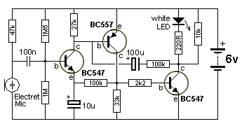
CONSTANT VOLUME HEARING AID
We mentioned at the beginning that you cannot force conditions on the
base of a transistor.
Here is a circuit that automatically adjusts the voltage on the base of
the first transistor and this effectively changes the gain of the
transistor to produce a constant volume, no matter how loud or quiet the
surroundings. 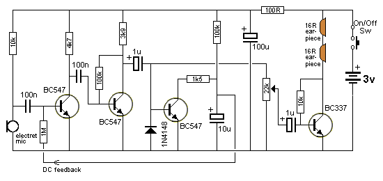
When the circuit is quiet the transistor is not turned on at all
and the 10u is charged via the 100k resistor. This put a voltage on the
feedback line to the base of the first transistor.
The circuit is now very sensitive and will pick up the slightest sound.
This faint sound will pass through the first two stages and into the
base of the third transistor.
If you don't follow my reasoning on SEEING A TRANSISTOR AS A
VARIABLE RESISTOR, how are you going to design this type of circuit:
The transistor receives Infrared light from a LED and the resistance
between the collector and emitter leads reduces to a point where pin 5
of the microcontroller sees a low of less than 1.3v
The characteristics of the IR transistor are: 1M in darkness and
10k or less when detecting IR light.
But this circuit not very sensitive with the 10k collector resistor and the IR LED has to be very close
to the IR transistor for the microcontroller to register a LOW. .
How do you improve the sensitivity?
The IR transistor does not have a base lead, so all your theory about
biasing the base of a transistor is worthless. It does not apply. 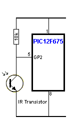
The IR transistor can on be turned on by the IR light and when it is
turned ON by very bright light, the resistance across the
collector-emitter leads is 10k.
The voltage divider becomes 10k in series with 10k and the voltage at
the join is 2.5v. This is not LOW enough for the
microcontroller to register a LOW and the circuit DOES NOT WORK.
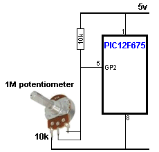

If the 10k LOAD resistor is connected across the power rails, it will
pass twice the current. But if the LOAD resistor is connected to a
voltage that is HALF the 5v supply, it will take half the current. This
current is the same as the capability of the IR transistor and so, when
they are connected in series, they drop the same voltage across each
component. That's why the lowest voltage in the first circuit is 50% of
rail voltage or 2.5v.
If the IR transistor tries to "pull down" the 10k LOAD resistor, it will
want more current from the circuit and the IR transistor cannot pass
this extra current and so the two remain at 50%.
If the 10k LOAD is replaced by 100k LOAD, the current through the 100k
when connected across the power rails is a lot less than the capability
of the IR transistor and so the transistor will be able to "pull down"
the 100k until the current wanted by the 100k is equal to the capability
of the IR transistor. The transistor is capable of "pulling it down"
to almost the zero volt rail and we are not going into the exact value
but it is low enough for the microcontroller to detect a LOW.
A lot more enlightening discussions and concepts can be found
HERE.
https://www.talkingelectronics.com/projects/TheTransistorAmplifier/TheTrAmp/TheTrAmpP1.html
More on the Transistor Amplifier can be found
HERE.
https://www.talkingelectronics.com/projects/TheTransistorAmplifier/TheTransistorAmplifier-P1.html
100 Transistor Circuits can be found
HERE.
https://www.talkingelectronics.com/projects/200TrCcts/200TrCcts.html
https://www.talkingelectronics.com/projects/200TrCcts/101-200TrCcts.html
After you read and study and understand what I have produced, you will
be able to design many types of circuits. These are called
BUILDING BLOCKS and by connecting blocks together you create circuits
that do magical things.
Contact Colin
Mitchell if you want any help
Let me know if I have missed a spelling mistake or forgotten something.
I am proof-reading things all the time and this has reached more than 10
revisions. It takes an enormous amount of brain-power to write technical
explanations and that's why no-one has gone into the depths of
describing the technicalities of circuit-design.