|
THE POWER SUPPLY |
Headings in this 2-page article:
Adjustable Output Voltage
Boost Regulator
Buck Regulator
Capacitor Supply
Constant Current Supply
Doubler - via Full Wave Voltage Doubler
Dummy Load
Fault Finding
Full-Wave Rectifier
Half-Wave Rectifier
How Capacitors (electrolytics) work in a Power Supply
Impedance - why the impedance of a power supply must be as low as
possible.
Negative Supply
Plug Pack
Plug Pack Regulator - a construction project
Positive and Negative Supply
Regulation - the importance of good regulation
Resistive Power Supply
Ripple Factor
Simplest power supply
Testing A Power Supply
Transformer
Transformerless Power Supply
Transistor Series Regulator
Transistor Shunt Regulator
Voltage drop 0.7v
Voltage Doubler - via Full-wave Voltage Doubler
Voltage Multiplier
Zener Diode Regulation
3-Terminal Regulators
One of the most important sections of a project is the POWER SUPPLY. It
will determine if everything works correctly. It is simply the
most important part.
A power supply is also called a PSU (Power Supply Unit)
or Power Supply Module.
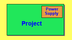
All projects need a Power
Supply
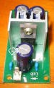
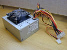
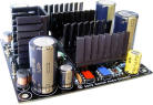
Power supplies come in all different sizes, from very simple to extremely complex:
 |
 |
 |
 |
Quite often, we don't realise how important they are.
Some projects work on batteries, some from a plug pack and some from the
mains. We just turn them on and expect them to work.
But what about the thought that has gone into designing a power supply?
It's an art to design a good power supply and it's a specialist field. Some
companies concentrate only on power supply design, from a 1watt
potted device to an un-interruptible power supply of several kilowatts.
The simplest power supply is two cells connected to a project. We will
start with this and show
the thought that goes into designing it.
The correct design of a power supply requires an understanding of many terms
and we have discussed some of them on the previous pages of this course.
Those terms
will now be needed.
Fortunately a number of chips and modules have come on the market to make
designing a power supply a lot easier and one of the handiest components is the plug-pack.
It is simply a transformer in a plastic box with a plug on the side so it
can be plugged directly into a power-point. This saves dealing with the
mains voltage and provides guaranteed insulation.
But the biggest problem with a plug-pack is its "over-rating."
They do not supply the current stated on the label and don't make a very
good device for powering a project. However with the advent of regulator
chips, plug packs can be used very successfully.
That's why you need this discussion. You need to know how to interface a
plug pack to a project and lots of other things relating the absolutely
beginning of designing a power supply.
The first thing you need to understand is the meaning of IMPEDANCE. It is
the most important feature of a power supply. It is the same as the
"strength" of a bridge or skyscraper.
IMPEDANCE
A power supply must have low impedance.
By this we mean:
A power supply must have low-resistance components in the CURRENT PATH. The
current path starts at
the 0v rail, through the secondary winding of the transformer, through the
diode and regulator (or transistor) and through any resistor on the
positive rail. This path supplies the current and any component with a high
resistance will create a voltage-drop across it (when the high
current flows) and the output voltage will be reduced.
The following shows the "current-path" we are discussing:
The Current Path
This is the path to look for when servicing a power supply. It is the path
that will pass (deliver) the current.
Between the positive and negative rail we need a high-value electrolytic to
reduce the impedance of the power supply even further.
Electrolytics reduce the impedance
of a power supply
An electrolytic is similar to a shock-absorber in a car. Without a
shock-absorber, you will be able to push say the front-left part of a car
up and down in a "bouncing" motion. This is the same as the output rail of
a power supply. When the electrolytic is added, the rail does not move up
and down. The electrolytic also adds to the ability of a power supply to
deliver a high current. It is really an amazing component.
If a power supply cannot deliver a high current, the
voltage on the output will drop and this can cause distortion or
faulty operation of the rest of the project.
THE SIMPLEST POWER
SUPPLY
The simplest power supply is a cell or battery. A cells is either 1.5v (or
3v). A battery is a number of cells.
The term IMPEDANCE still applies and the CURRENT PATH is though the cell or
battery.
The current path
A new cell or battery has a low impedance as proven by its ability to
deliver a high current.
As the battery gets older, the voltage across its terminals reduces and the
maximum current it can deliver also reduces.
The reason is the active chemicals get used up, and the resistance of the
by-products is higher.
All projects work perfectly with a new battery, but unless you remember
some simple rules for correct designing, a new battery can still cause problems.
When deigning high frequency projects such as 100MHz "bugs" or FM
transmitters, the leads to the battery must be as short as possible to
keep the impedance of the power supply LOW.
Here is an example:
This FM transmitter circuit does not work:
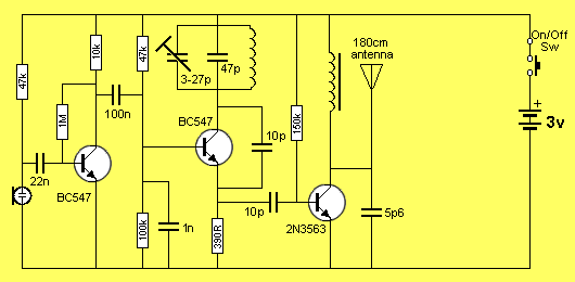
The 3v supply is too far from the circuit. The circuit is operating at
approx 100MHz and the power-rail is moving up-and-down at this frequency
and becomes an ANTENNA! It begins to radiate electromagnetic waves
and in the process becomes a HIGH IMPEDANCE line.
In other words it becomes a high resistance line and a voltage develops on
it that opposes the 3v supply.
The current reduces and the circuit does not get the required energy from
the battery.
This is equal to the power supply having a HIGH IMPEDANCE.
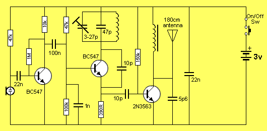
The impedance can be reduced by adding a capacitor across the power rails.
The performance of the following circuit will improve:
By placing the 3v supply very close to the circuit, the performance will
increase enormously:
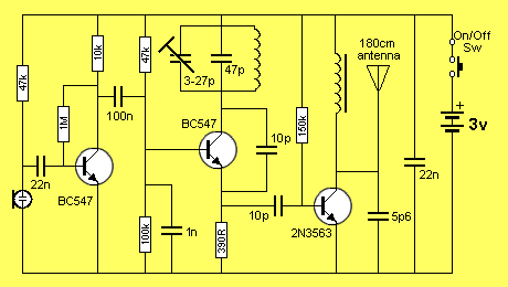
To keep the impedance of a power supply LOW, we need to:
(a) Add an electrolytic - for low-frequency circuits,
(b) Add a capacitor - for high-frequency circuits, and
(c) keep the leads short.
Keeping the impedance LOW
HOW THE CAPACITORS WORK
The capacitor or electrolytic
across the battery is effectively a miniature battery with a very low
internal resistance and is capable of delivering a very high current for a
very short period of time.
When the project does not require a high current, the rail voltage is a
maximum and the electrolytic or capacitor charges.
When the project requires a heavy current, the rail voltage drops slightly
and the voltage across the electrolytic is higher and it begins to deliver
its energy to the rail.
An electrolytic takes time to charge and discharge so it is only suitable
for low-frequency fluctuations. A ceramic capacitor can be charged and
discharged at a high rate and thus it is suitable for high-frequency
fluctuations. By adding both to the power rail, we cater for the full range
of frequencies.
0.7v DIODE DROP
Next we can add a diode to convert a 6v supply to
5.3v.
TTL chips require a 5v supply and will operate up to a maximum of 5.5v.
The following circuit shows a diode added to the positive rail.
A "normal" power diode drops 0.6v to 0.7v when it is conducting. This is
called the "characteristic" voltage drop of a diode.
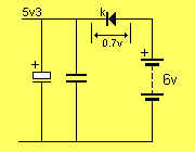
Adding a diode to produce a 5.3v rail
The diode also provides protection from reverse voltage:
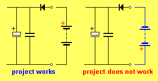
Reverse-voltage protection
If you need the full battery voltage to be delivered to the circuit, the diode can be placed as shown and a fuse added. If the battery is connected incorrectly, the fuse will blow.
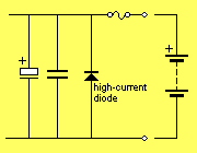
Reverse-voltage protection
ZENER DIODE REGULATION
The simplest regulator is a zener diode. It is called a SHUNT REGULATOR as
it goes directly across the power rails. It
is a very wasteful way to produce a steady voltage.
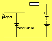
A zener diode shunt
regulator
With a zener diode shunt regulator, current is
flowing through the zener at all times and this is wasted current. If the
main circuit requires no current, the zener consumes all the current.
If the
main circuit requires a small amount of current this current actually comes
from the zener. In other words the zener takes slightly less current and
this current is exactly the amount required by the main circuit.
The zener works like this: When the main circuit starts to take a small
amount of current, this current flows through the dropper resistor. This
causes a slightly higher voltage to appear across the dropper resistor.
This means the voltage across the zener is slightly less.
When the voltage across the zener is reduced slightly, the zener "turns
off" a small amount and it allows slightly less current to flow through
it.
This current is exactly the same amount of current required by the main
circuit.
The same amount of current is always taken from the battery, it just gets diverted
from the zener to the project. The following diagram shows how the current
is divided between the load and the zener:
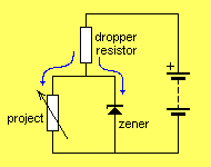
The current is divided between
the project and zener
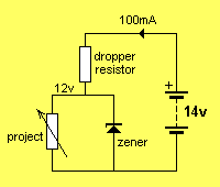
A zener diode is only suitable for small values of current.
It works like this:
If a project takes 10mA when idle and 100mA when processing a signal, the
range is 90mA.
If the rail voltage is 12v, the zener will be required to pass 90mA when
the project is idle and 10mA when operating.
The wattage rating of the zener will be 12 x 0.9 = 1.08watt.
Use 1watt zener.
If another project takes 350mA @ 12v when idle and 440mA when operating,
the difference is 90mA and the same zener can be used.
The dropper resistor also represents waster power and its value is worked
out as follows:
The resistance of the
dropper resistor
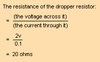 The
wattage = V x I = 2 x 0.1 = 200mW
The
wattage = V x I = 2 x 0.1 = 200mW
TRANSISTOR SHUNT
REGULATOR
In place of the zener diode we can use a transistor. It is still the same
wasteful design but the rail voltage can be set via two resistors and this
saves stocking lots of different voltage zeners.
You will notice, we are adding components to create
improvements to power-supply designs and this is the best way to
understand how a power-supply works.
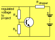
A transistor shunt regulator
The analysis and design of the circuit above starts with resistor Rb.
When the voltage across this resistor reaches 0.65v, the transistor starts
to turn on and pull the regulated rail to the desired voltage.
In other words, the only two critical values are: the value of Rb and the
characteristic voltage between the base and emitter of the transistor
(0.65v).
Nothing else matters! Isn't that a surprise!
Once you know the secret of where to begin, things start to make sense.
Now we come to the skill of working out the value of Ra and Rb to produce a
voltage of 0.65v at the join.
Suppose we require 5v for the regulated rail.
We have the following circuit:
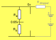
The voltage-divider Ra:Rb
To work out the value of Ra and Rb, we need to know the current flowing
through the voltage divider. This is a technical decision. In other words
you have to decide what current you want to flow through the divider.
Theoretically it can be ANY VALUE. That's right, it can be any value
above a certain minimum. To arrive at the minimum value we need to know the current
flowing through the regulator transistor (we will assume 100mA).
If the gain of the transistor is 100, the base current needs to be 1mA.
This means 1mA must flow through Ra.
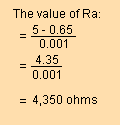
This value is non-standard.
Use a standard value. Select 3k9.
The value of Rb:
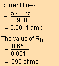
Use a 560R and 33R in series.
The final circuit:
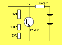
The transistor shunt
regulator circuit
An improved transistor regulator is the:
TRANSISTOR SERIES REGULATOR
The series transistor regulator is a more-efficient design and caters for a
high current load and wide fluctuations.
It wastes almost no energy when no current is being taken by the project
but the transistor must be heat-sinked when a high current is required.
A simple series regulator is shown in the diagram below.
It is effectively an EMITTER-FOLLOWER:
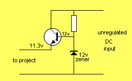
Simple series transistor
regulator
The emitter of the transistor "follows" the base and is approx 0.7v below
the base.
The base is fixed at 12v by the zener diode and the voltage to the project
is 12v - 0.7v = 11.3v
THE TRANSFORMER
There is not a lot you can do about designing a transformer.
They are "off the shelf" components and you have to take the manufacturers
specifications as accurate. But they are often misleading. Especially with
small transformers (5VA to 30VA).
The size of a transformer indicates its VA rating (volt-amp rating).
There are basically three types of transformers:
1.The square-looking type made from "E's" and "I's" (or a solid ferrite
material).
2. The toroidal-type, looking like a large doughnut and
3. The
enclosed-type called a pot-core.
There are lots of variations and shapes,
such as elongated-types to fit certain spaces or inductor-types that look
look a choke.
But we will concentrate on three types and two different
frequencies of operation.
The "E" and "I" type is used for low frequency (50 - 60Hz) and the ferrite
type is used for high frequency (50kHz - 1MHz).
But the big problem is the
data provided
with some of them - especially "plug packs."
Some transformers are rated at 500mA, while some
smaller types claim to be 500mA. This is an error and you have to be
aware of false identification.
The VA rating of a transformer depends on its size in each category ("E"
and "I" - toroidal and high frequency).
There is no "super transformer" that is 50% better than the others in the
same style and you can accurately go by size, shape and weight for each
category.
The largest and heaviest transformer (per VA) is the "E" and "I" type. The
toroidal will deliver about 200 -300% more (watts) for the same
weight and the high-frequency ferrite types will deliver 6 times to 10
times more (watts).
There are three types of secondary winding:
It can be a single winding, centre-tapped or
two separate windings.
You can use a single diode for half-wave rectification or 2 diodes for
full-wave from a centre-tapped secondary or 4 diodes in a bridge for
full-wave rectification.
Half-wave rectification is very inefficient and is no longer used.
Full-wave is the best design.
The centre-tapped secondary was designed many years ago to get around the
problem of PIV rating for diodes (see below).
The centre-tapped secondary (and 2 diodes) is not as efficient as a
single secondary winding and 4 diodes because with the centre-tapped
secondary, each winding is only delivering energy for a half-cycle and
this means only half the volume of the secondary space of the
transformer is being used. This means the secondary winding is thinner
and has a higher resistance and higher copper losses. The only saving is
the cost of 2 diodes.
The full-wave voltage doubler was also designed many years ago as a
low-cost way to generate a high voltage for the accelerating anode on a
Cathode Ray Tube.
Here are 4 different ways to connect to the
secondary of a transformer:
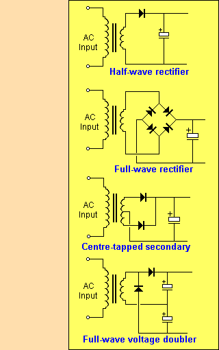
There are a number of reasons why four different circuits were designed.
In the early days of electronics, power supplies were designed to meet
the requirements of valve amplifiers and these required a plate voltage of
285v or more. In the full-wave circuit, the PIV
(peak-inverse-voltage) rating for each diode must be equal to at least
twice the peak load voltage and since this was higher than some of the
diodes in the early days, a number of alternatives were
produced - such as the centre-tapped secondary.
The full-wave voltage doubler circuit was very clever as it produced a
smoothed DC output from a low voltage winding. It was much cheaper to wind
a lower-voltage winding as it had fewer turns of thick wire.
All these "clever designs" are now no longer needed as the voltage
requirements of modern electronics is much lower and regulation is provided
with IC's.
The only design you need to study is the Full-wave rectifier. All
modern power supplies use a single secondary winding and a bridge rectifier
(four diodes in a block that looks like a chip).
THE HALF-WAVE RECTIFIER
The half-wave rectifier produces a waveform with a very large AC
component called "ripple" and requires a lot of smoothing to make
it acceptable for electronic circuits. By adding 3 more diodes in
a "bridge"
we can get "full-wave" rectification and this requires less
smoothing.
For this reason the half-wave rectifier is no longer used.
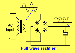
THE FULL-WAVE RECTIFIER
The full-wave rectifier delivers both the positive and negative
part of each cycle to the input of the "electronics."
When we talk about a "full-wave rectifier" we mean the "bridge
rectifier" made up of 4 diodes:
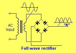
Two diagonally-opposite diodes pass the
waveform to the output line during one half of the waveform and the other
two diodes pass the signal to the output during the second half of the
waveform.
At point "A", an electrolytic smoothes the pulses by
charging and discharging at the appropriate times to create a
fairly smooth waveform.
It is very important to make this waveform as smooth as possible
(with the aid of a large electrolytic) as the "electronics" (the
regulator) will improve the "smoothness" 1,000 times or
more and if it starts fairly smooth, the end result will be very smooth.
The smoothing effect of the
electrolytic
FULL-WAVE VOLTAGE
DOUBLER
The full-wave voltage doubler circuit is shown in fig 1:
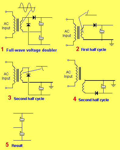
Although this type of
circuit is rarely used as the power supply in modern circuits,
its principle is very interesting and is the basis of
voltage-multiplying circuits such as quad multiplying and even
increasing voltages 10 times for devices such as fly-zappers, ozone and
ion generators to flocculate (remove by dropping or falling to the
floor) dirt and dust particles from the air. These are all very
effective for the job they are designed for and that's why they
are still in production. In fact the ozone producing circuit is
extremely
effective at removing smells and dangerous bacteria in toilets as it
kills all bacteria but the gas is so corrosive it destroys all metals
except gold.
The full-wave voltage doubler is very efficient because it uses both half-cycles
of the voltage-waveform. In addition only two diodes are needed and two
electrolytics. The secondary winding needs only half the number of turns
of a thicker wire and this is cheaper to produce. The output of the
power supply is a fairly smooth voltage that has been doubled. A lot of
advantages with very few parts.
Once you understand the principle of how the voltage doubler works, you will understand
triplers and quad multipliers etc.
Fig 1 above shows the complete circuit.
The top electrolytic is charged to a peak voltage when the voltage rises during
the first half cycle of the AC waveform. This is shown in the fig 2. When the voltage falls from the peak-value towards 0v rail, the lower
electrolytic starts to get charged. This is shown in fig 3.
To make is easy to see what is happening, we have connected the bottom
winding of the transformer to ground. This will make it easy to see how
the voltage charges the lower electrolytic. This is not done in a real circuit
as the result would be a positive voltage from the top electrolytic and
a negative voltage from the lower electrolytic.
When the voltage from the transformer reverses, you can see the bottom
of the winding cannot move as it is tied to ground and thus the top of
the winding produces a negative voltage. This negative voltage will not
pass though the top diode and it will only pass though the lower diode
to charge the lower electrolytic.
In figure 4 we have moved the secondary winding to below the 0v rail to
show how it charges the lower electrolytic. This charging only takes place during
the time when the waveform increases from 0v to a peak in the negative
direction.
Remove the temporary earth and we have two fully charged electrolytics.
This is shown in fig 5.
Each electrolytic will be charged to the peak value of the secondary of
the transformer.
Since the two electrolytics are in series, the combined voltage will be
double the peak of the transformer.
That's how the VOLTAGE DOUBLER works. Each electrolytic is charged
via a half-wave circuit but the transformer is delivering energy during
each half cycle and that's why the circuit is called a FULL WAVE voltage
doubler.
FULL-WAVE VOLTAGE MULTIPLIER
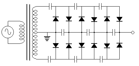
HALF-WAVE VOLTAGE
MULTIPLIER
Most voltage multiplier
circuits require very low current for their operation. They are used for
their high voltage as a high voltage produces some amazing effects. For
instance, if a high voltage (above about 5kV) is connected to a pin with
a sharp point, a spray of electrons will fly off the point and produce
an "electric wind." These electrons will accumulate on dust particles
and drop them to the ground.
This is the principle of an electrostatic precipitator. If the voltage
is increased further, ozone gas (O3) will be produced -that's
why the voltage must be below about 15kV to avoid ozone being produced.
This is the most corrosive gas known.
Cattle prods and insect zappers also use voltage multiplying circuits
and these require a high voltage with very little current.
That's why a half-wave circuit can be used. It uses less components than
full-wave but produces a lower current.
The principle of a voltage multiplying circuit is amazing. It charges
capacitors in parallel and allows them to discharge in series.
Thus is something you cannot do with batteries - charge them in parallel
and allow them to discharge in series to deliver a high voltage - so
let's see how this is done.
Figure 1 shows the complete Voltage Multiplier circuit:
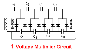
We will take the operation of the circuit in
slow-motion and show how each capacitor charges. Once they are all
charged, they get topped-up during each charging-cycle and the
voltages are slightly different to the start-up cycles.
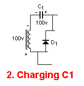
We will start with just C1. It is uncharged.
We start when the secondary winding has a peak of -100v at the top of
the winding. This is to
create a voltage on C1 as shown in fig2. If the secondary winding starts
with +100v at the top of the winding, the capacitor will get charged in the
wrong direction and this will be corrected
during the next half-cycle, as the capacitor must be charged as shown in
fig 2.
All the other components in the circuit have been removed as they
are not involved during this instant. The voltage across D1 is
almost zero and you can consider the positive of the capacitor to be
connected to the + of the secondary winding. This means none of
the rest of the circuit is receiving any energy.
The voltage on the secondary winding now changes direction and it pushes C1 "high in the air" by an amount of 100v as shown in fig 3. C1 has about 100v on it and some of its energy is passed to C2. This is an important concept to understand. C1 is like a 100v battery. It is 100v but it has very little energy. When you put a 100v battery on top of 100v winding from a transformer, it produces a voltage of 220v, but the capacitor energy is very small and as it passes some of its energy to C2, its voltage decreases.
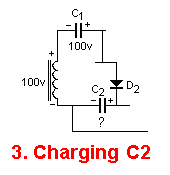
100v from the winding is a "strong" voltage and does not change. What happens is the energy of 50v from C1 is delivered to C2 as well as 100v from the secondary winding, to produce the final voltages as shown in fig 4:
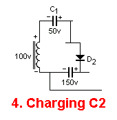
The voltage on the secondary of the transformer reverses again and this action charges C1 to 100v:
When the voltage reverses again, the voltage on C2 is increased from 150v to 175v:
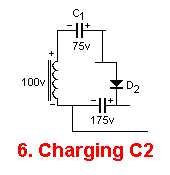
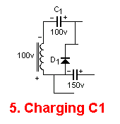
As you can see, each half-cycle C1 is topped up to 100v and it delivers energy to C2 and eventually C2 will rise to nearly 199v.
C1 does not actually increase the voltage on C2 by the amount in the
steps above because the circuit has other capacitors that are charging
at the same time but concept still holds true. The energy from C1 is
passed to C2 until the voltage on C2 is about equal to the voltage of
the winding plus the voltage on C1.
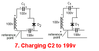
Let's explain how diode D2 disappears and diode D1 comes into operation.
In the first diagram of fig7, the winding is producing 100v. This is a
peak voltage and only appears when the waveform is at the top of its
excursion (the top of its cycle). As soon as the waveform starts to
decrease, the capacitor drops down too and the positive end of the
capacitor drops to 199v, 198v, 197v . . . .
When this voltage drops below 198v, diode D2 drops out of conduction
because the anode end stops being about 0.6v higher than the cathode.
The diode only conducts current when the anode is about 1/2v higher than
the cathode.
The voltage from the secondary winding keeps dropping and at some point
these is zero voltage across the winding. At this point the capacitor is
about 100v above the reference point. Al this point neither diode is in
conduction and nothing is happening.
The secondary voltage keeps dropping and not the top of the winding is
an increasing negative voltage.
What we have is a winding trying to charge a 100v battery via a diode
and in fact the capacitor has only about 95v on it. AS soon as the
voltage on the winding reaches 95.6v, diode D1 cones into conduction and
current flows from the winding into the capacitor to charge it to nearly
100v.
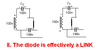
In the diagrams above, when diode D1 or D2 (or any of the diodes) are conducting, it is exactly like a link as nearly the same voltage is present on both ends of the diode (there is only a 0.6v difference). This means the diodes in fig 7 can be changed to:
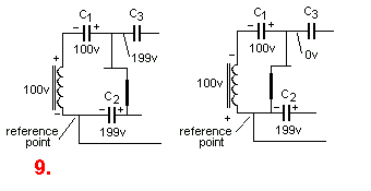
You can see the voltage on
the left side of C3 is 199v in the first diagram of fig 9 and 0v in the
second diagram. This is just a point to help you understand that voltages
are changing on parts of the circuit that you were not aware of.
The main thing to note is the 199v on C2.
Charging C3:
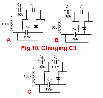
Fig 10 shows how C3 is charged from C2. In diagram "A" the voltage on C2
is passed to C3 and this voltage gradually increases as shown in figures
2, 3, 4, 5 and 6 above. It may take quite a few cycles to get to 198v
but eventually C3 will reach 198v as shown in diagram "C."
During the part-cycle when C2 is charging, the diode shown in the
diagram(s) is reverse biased and the voltage on C3 is not affected. The
main point to note is: C2 charges C3.
We now add C4:
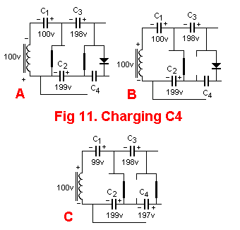
In Fig 11A we see C2 charging C3 and the two diodes connecting the two
capacitor can be considered as links to make the concept easier to see.
When the voltage on the secondary winding is reversed, as shown in
drawing 11B, C3 charges C4. This is easy to see in 11C by turning the
diodes into links.
We now add C5:
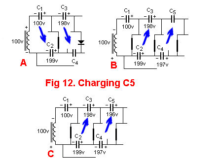
In the first half-cycle, as shown in fig12A, C1 charges C2 and C3 charges
C4. When the voltage in the secondary winding reverses, the secondary
winding tops up C1 and C2 charges C3 and C4 charges C5.
Each capacitor "down-the-line" gets charged to a slightly lower voltage
and this is the best the circuit can do. If a current is drawn from the
output, the voltage on each capacitor reduces even more.
Up to about 10 stages can be used and you can see the final voltage by
adding the voltage across each capacitor.
REGULATION
Regulation is one of the hidden words in power supply design.
It applies to both the output voltage of a power supply and a transformer.
When referring to a transformer, it is its ability to deliver a fixed voltage, over a wide range of current.
It is impossible for a transformer to maintain a constant output voltage when a load is applied as the secondary winding has a resistance (impedance) and the flux density changes.
The loaded voltage of some transformers can drop as much as 20% - 50% and unless there is a circuit to compensate for the change, we will get "hum'" "ripple," "drop-out" and faulty operation of the project.
To get around this voltage-drop, manufacturers add extra turns to the secondary and deliver a higher "no-load" voltage.
This means some transformers will produce 16-18v on no-load and drop to 12v when full current is being delivered.
The maximum voltage for CMOS chip is 16v and they will be damaged if supplied with 18v.
We need a circuit to take the 18v and convert it to a fixed voltage - preferably 12v or less.
The circuit is called a REGULATOR.
A regulator has the amazing ability to convert a high voltage to a low voltage and maintain it accurately over a wide range of current requirements - even when the input voltage is rising and falling.
There are two types of circuits:
Type A provides a constant voltage from a higher supply voltage.
For instance, a 7805 will provide a constant 5v, from a supply of 8v to 20v.
If the supply drops below 7v, the 5v rail will drop.
The Type A circuit can use a REGULATOR in the form of a component that looks like a power transistor:
It actually contains more than 30 transistors and requires only a
few external components to create a complete power supply. Basically it
operates by chopping the input voltage and delivering small amounts to the
output. It is
called a 3-terminal regulator or linear regulator.
Type A
circuits can also use switch-mode arrangements
in which the output voltage is created via an inductor. The output
voltage is entirely created by the energy from the inductor.
Type B circuits provide a constant voltage from a lower supply voltage.
This is called a step-up regulator. The voltage can be produced by charging
a capacitor and placing this voltage on top of the rail voltage or it can be produced by passing a current through an inductor then turning
it off and allowing the inductor to collapse and produce a high
voltage. In all cases, the output voltage is monitored and accurately maintained.
That's why all these circuits are called REGULATED POWER SUPPLIES.
3-TERMINAL REGULATORS
- also called Linear Regulators
The common name given to "chip" regulators is "3-Terminal Regulators."
This has made designing power supplies very easy. Simply add a 3-terminal
regulator and a few surrounding components and you have a regulated power
supply.
But there are some hidden secrets.
The most important fact to remember is to prevent the regulator dropping
out of regulation.
This means the input voltage must be 3v higher than the
voltage you are delivering.
With very poor quality plug-packs, this can be quite a problem. They can drop below
the required voltage when drawing a current. This will cause problems with the project and be very
difficult to detect - unless you are aware of the problem!
3-terminal regulators work on the principle of delivering energy to the
output in pulses.
When they are turned on, the voltage drop across the regulator is low and
the heat generated is small. When they are off, the heat generated is
zero.
In this way they can produce an accurate output voltage and high current
demand, with minimal losses.
A typical 3-terminal regulator power supply is shown in the following
diagram:
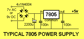
There are four important points to remember when designing a power supply:
1. The regulator must be close to the edge of the board so it can be attached to
a heatsink.
2. The heatsink must also be attached to the PC board so that is does
not move and allow the leads of the regulator to break.
3. The 2200u and both the 100n monoblocks must be mounted close to the regulator.
4. The input voltage must be higher than the output to allow for the
voltage drop across the bridge and regulator. The minimum for a 5v output is 7v
AC or 9v DC.
Note: It does not matter which way around the AC or DC supply is connected to
the bridge as the bridge will automatically adjust for either polarity. This is
one of the advantages of placing a bridge on the input of a project. It allows
either-way connection to power the project.
INCREASING THE
OUTPUT VOLTAGE
The output voltage of a supply can be increased by "jacking up" the
voltage produced by the 7805. The way the 7805 works is this: It maintains a voltage
of 5v between output and common terminal. If the voltage on the common terminal
is increased (jacked up), the output voltage will be 5v higher. The 7805 always
maintains 5v between output and common. The
circuit below produces an output of 12v.
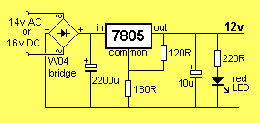
Almost any voltage
between 5v and 30v can be obtained by this method. This saves stocking the
complete range of regulators.
The output voltage is determined by two resistors in VOLTAGE DIVIDER MODE. Five
volts is always present across the 120R resistor and if another resistor is
placed in series, it will have a proportional voltage across it. In the circuit
above, 7v is developed across the 180R resistor, making a total of 12v on the
output.
To increase or decrease the voltage, only one resistor has to be changed in the
circuit above. The 120R is retained and the 180R is changed. If it is increased to 220R, the output voltage will be 14v, for a 330R, the output voltage will be 18v. The resistor in the common line
can be a potentiometer. This will produce an adjustable output
voltage. The dropper resistor for the LED will also have to be
increased so the LED is not over-driven on the higher voltages.
A meter can be placed on the output to monitor the voltage and current taken by
the load.
There is only one problem with an adjustable supply. The regulator
must be heatsinked so it is capable of dissipating the heat for the worst condition. In
addition, the input voltage must be sufficient to cater for the maximum
output voltage.
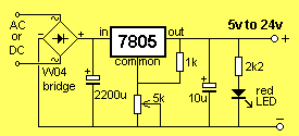
ADJUSTABLE OUTPUT VOLTAGE
The output voltage can be adjusted (varied) from 5v to 24v via a
potentiometer connected to the common line of the regulator. The input
voltage and heatsinking of the regulator must be sufficient for the output
voltage and current. The output may not deliver more than 100mA @ 5v due to
the heat produced by the regulator if the input voltage is say 24v - 36v.
This is one of the disadvantages of a variable power supply if this design.
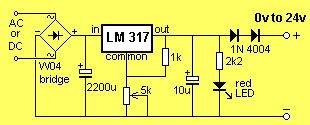
THE LM 317 REGULATOR
The advantage of an LM317 regulator is the supply will go down to
1.2v. If you add two diodes (in series with the output line), the voltage will
go down to 0v as shown in the following circuit:
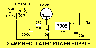
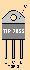
HIGHER CURRENT
If you require more than 1 amp, the 7805 can be
combined with other components to provide an output of up to 3 amps, with
the circuit below. The current is
switched through the TIP2955, so the 7805 can be run without a heatsink since it
only regulates the voltage. Note the 3-amp diodes in the power supply.
For currents greater than 3 amps, additional TIP 2955 transistors can be
"piggy-backed" on top of the TIP in the circuit. If the gain of each
transistor is approximately the same, the transistors will current-share the
load and get equally hot.
POSITIVE AND NEGATIVE SUPPLY
A positive and negative supply can be generated from a single bridge by using a centre-tapped
transformer:
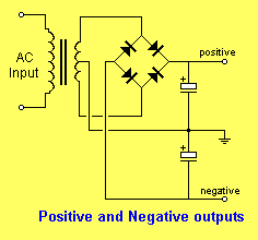
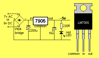
A NEGATIVE POWER SUPPLY
A negative power supply
can be produced with a 7905 voltage regulator. Three things to be remembered are:
1. Check the connections of the 7905 before fitting it.
2. Reverse the 2200u and 10u electrolytics and LED.
3. Reverse the bridge so the negative goes to the "in" pin
of the 7905.
100mA POSITIVE REGULATORS
3-Terminal regulators are available in 100mA
versions. They look like a small-signal transistor:
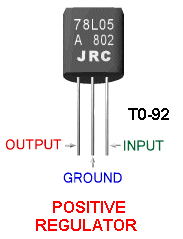
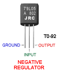
100mA NEGATIVE REGULATORS
3-Terminal regulators are available in 100mA
negative output versions. They look like a small-signal transistor.
Note: The pinout of the positive regulator is NOT the same as the
negative regulator. The circuit will not work if the wrong regulator is
fitted and the regulator can be damaged.
THE CONSTANT-CURRENT
SUPPLY
The voltage
regulator can be wired to produce a constant output current. This is not
suitable for some applications as many devices require a high current at
start-up (motors and globes) while others require a varying current (amplifiers)
for their operation.
However there are a few devices that need a constant current for their correct
operation and one device is the Laser Diode.
The actual current requirement depends on the output of the diode and a standard
1 milliwatt type requires between 70 and 100 milliamp.
The characteristic voltage developed across the diode is less than 3v so that a
3-terminal regulator that goes down to 1.2v will be needed.
HOW THE CIRCUIT WORKS
By simply connecting a resistor between the output of the regulator and the
load, and taking the common or "adj" terminal as shown below, the
output current can be set by the value of the resistor.
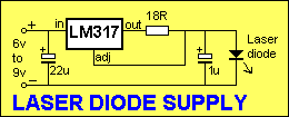
It
works like this: No current "comes out" the adjust terminal. It is a
"sense" line. It merely acts as the 0v reference line for the
regulator. The only side issue is the current taken by the regulator flows
through the adjust line and this is approximately 10mA. But in our discussion,
this is ignored.
The voltage between the output terminal and "adjust"
is fixed a 1.2v (for this type of regulator). The 18R resistor in the circuit is
called a voltage dropping resistor. It is designed to produce a voltage across
it according to the current flowing.
If it is 18R, the current flow will be: 1.2/18 = 66milliamps. If the resistor is 10R, the
current needed to produce 1.2v across the resistor is: 1.2/10 =
120milliamps. If we choose 15R, the current flow will be 1.2/15 = 80milliamps.
The laser diode in the example above requires a current between 70milliamps and
100 milliamps. You can choose 15R or 18R for the voltage-dropping
resistor.
How the 3-terminal regulator keeps the output current constant, even if
the input voltage is increased:
Firstly, the current through the "common" or "adj" lead is
only about 10mA and this will not come into the discussion.
If the input voltage is increased, the output voltage will (may) increase and
this will allow the load (the laser diode) to take more current. The increased
current through the 15R or 18R resistor will increase the voltage across it and
this will be detected by the circuit inside the regulator. The circuit will
"turn down" the output voltage and everything will be stabilised.
This type of circuit is needed to drive a laser diode from a battery supply. As
the voltage drops, the constant-current circuit maintains the same
current.
If the constant-current circuit is not included, the current to the laser diode
would drop as the battery voltage falls and the laser diode would cease to
operate if the current falls below a certain minimum.
All "Laser Pointers" have an inbuilt constant current circuit
to maintain the operation of the laser.
The output
current in the following circuit is determined by the value of resistor
R.
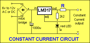
The input voltage must be at least 5v above the output voltage. This is due to the fact that the regulator need aout 4v between the in and out terminals so the components inside the regulator will perform their function plus 1.2v across resistor R. The brightness of the indicator LED will depend on the voltage being supplied to the load. It does not indicate the current being delivered. Use the table below for the following currents:
|
Output Current |
R |
|
50mA |
24R (use 18R or 27R) 12R (use 10R + 2R2) 8R (use 8R2) 6R (use 5R6) 2R4 (use 2R2) 1R2 (use 1R) |
RIPPLE FACTOR
One characteristic of an electrolytic is rarely mentioned.
It is RIPPLE FACTOR.
This is the amount of current it is able to deliver without
getting too hot.
It is one of the factors that determines the size of the electrolytic and
since everything is being miniaturized, the Ripple Factor suffers.
If the size of the electrolytic is too small, it will warm up during its operation and
dry out. The capacitance will reduce
and all sorts of
faults will develop.
One way to determine the suitability of an electrolytic is to feel it after
the supply has been operating for a while. It it is hot, you can be sure it
will suffer from overheating.
On the other hand, if it is cold, it could be dry.
One of the problems with the
3-terminal regulators described above is the fact that they are not very efficient and tend to get fairly hot.
A better design is a switching power supply using a switching chip plus an
inductor or capacitor to produce the output voltage and current. This
design is more efficient and has the ability to produce
an output with a higher voltage or current than the supply (but not both at
the same time!).
There are two types - Buck and
Boost.
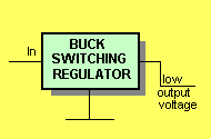
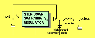
THE BUCK REGULATOR
The Buck regulator requires a high input voltage and delivers a low voltage.
It is called a BUCK CONVERTER, BUCK REGULATOR, STEP-DOWN CONVERTER or
STEP-DOWN SWITCHING REGULATOR.
A switching regulator, when in the buck mode, produces a voltage lower than
the "in" voltage.
Buck switching-regulators have an internal high-frequency oscillator that turns a transistor
(or FET) on and off
and delivers bursts of energy to an inductor. When the transistor turns
off, the energy from the inductor is stored in a capacitor.
It will maintain an extremely stable output voltage (with a sensing line
that monitors the output) even
though the current required by the project may fluctuate and the input
voltage may rise or fall.
Buck switching regulators are available in 100mA, 1A, 5A plus other
values.
A buck switching regulator will take 12v @ 500mA and convert it to 5v
@1Amp. In other words it will take a high voltage at low current and
convert it to a low voltage at high current.
A step-down switching regulator chip requires only a few external
components to create a complete supply. Some of the components in the
diagram below are inside the chip.
A sense line (not shown) is connected to the output to monitor the voltage
and maintain stability.
An MC34063 IC in a step-down switching circuit:
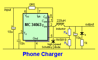
The output voltage is determined by the value (actually
the ratio) of Ra:Rb.
The chip has a 1.25v detector on pin 5 and when the voltage across Rb is
1.25v the chip begins to shut-down.
The output voltage:
![]()
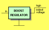
THE BOOST REGULATOR - the
step-up regulator
The BOOST switching regulator circuit has a low voltage
supplied to it and delivers a high output voltage. (The output current will
be lower than the input current)
It is called a BOOST CONVERTER, BOOST REGULATOR, STEP-UP CONVERTER or
STEP-UP SWITCHING REGULATOR.
Boost switching-regulators have an internal high-frequency oscillator that
turns a transistor on and off and delivers bursts of energy to an inductor.
When the transistor turns off, the energy from the inductor is stored in a
capacitor, via a high-speed Schottky diode
It will maintain a constant output voltage even
though the current required by the project may fluctuate and the input
voltage may rise or fall.
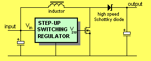
Boost switching regulators are available in 100mA, 1A, 5A plus other
currents.
A step-up switching regulator chip requires only a few external components
to create a complete supply.
Note: A boost regulator can produce a voltage higher or lower than the "in"
voltage.
The
MC34063 IC can be used in a circuit to produce a higher or lower voltage
than the "in" voltage.
SERVICING POWER SUPPLIES
Most faults in a power supply are due to the
electrolytics. They play a vital part in the performance of the
circuit and after a few years they can exhibit a lower capacitance due to
overheating and drying out.
When servicing a power supply the electrolytic is bridged with another
(WHEN THE SUPPLY IS TURNED OFF), to see if it is faulty.
Unusual effects can be created when an electrolytic dries out and the
quickest and cheapest thing to do is replace ALL OF THEM.
They can cause low output voltage, hum, ripple, hiccupping, distortion and
sometimes complete failure of the power supply.
The next component to check is the power supply IC such as the regulator or
control chip.
These are very reliable but can suffer damage if they are not heat-sinked
correctly.
Many of them have in-built thermal shut down if the
temperature rises excessively but if this feature is activated on a regular
basis, the chip will gradually suffer from over-heating.
Another problem can be a thermal fuse or low-value resistor. These
eventually suffer from heating and will fail. They are sometimes hidden in
a fibre-glass sleeve.
Don't forget to check the plug-pack as a smaller version may have been
substituted and will create all sorts of ripple problems.
Once you have covered these areas and the fault still persists, you will need to go to the
rest of the project and determine if it is taking more current due to the
fitting of additional devices.
CURRENT MEASUREMENT
It is very difficult to measure the current being delivered by a power supply.
If you insert a current detecting device, the additional resistance of the meter and leads will reduce the peaks. Even though the resistance of the meter is very small, the high current being taken by the circuit will cause a voltage drop to develop across the meter and the current peaks will be reduced.
That's why testing a power supply is very difficult.
Generally, there is very little to go wrong as it contains very few components, but when a fault develops, it can be quire technical.
This is due to the high currents and even short tracks on the PC board can introduce problems.
Make sure tracks have not burnt out and check the earth rail.
Sometimes a long earth rail will introduce problems.
For instance, a dry electrolytic on one of the rails may create a fault in a particular section that causes a low frequency hiccup and this is referred back to the power supply via another section.
Remember, a power supply is a LOW IMPEDANCE module and once this impedance is altered, a number of faults can develop.
Impedance is a very difficult thing to measure as it made up of so many factors.
That's why you have to use your skills when designing and servicing.
Don't forget to include 100n ceramic capacitors near the input and output of a 3-terminal regulator. They prevent it self-oscillating.
Make sure the tracks to a 3-terminal regulator are thick to reduce the impedance.
And make sure the 3-terminal regulator is adequately heatsinked.
HEATSINKING
One of the important points to remember is heatsinking the power supply regulator.
The amount of heat generated by a 3-terminal regulator depends on two factors:
1. The current being delivered to the project, and
2. The voltage delivered to it via the transformer or plug-pack.
We will take this simple example:
A 12v plug-pack is powering an audio amplifier project and the output is distorted.
The 300mA plug pack is replaced by a 500mA unit and the audio is perfect.
But the regulator gets hot and shuts down.
What is the problem?
The larger plug pack has better regulation. It is capable of supplying a higher voltage to the regulator - and thus a higher current.
The regulator is capable of maintaining a high rail voltage and the amplifier draws a higher current.
These two factors cause the regulator to dissipate a higher wattage and it heats up excessively.
The only solution is to increase the size of the heatsink.
CONCLUSION
This page has described power supplies up to about 1amp. These are cheap and easy to design as transformers, diodes and 3-terminal regulators are capable of delivering 1amp.
This is the absolute maximum current as low-cost diodes are rated at 1amp and a 1amp transformer is rated at one-amp AC! This is only 0.707amp DC as 12v AC becomes 16v DC and if you try to deliver 16v DC at 1 amp, the wattage will overload the transformer. It is not advisable to deliver more than 700mA on a continuous basis, for this reason. Many 1amp diodes are really only capable of delivering 700mA. When the current through these diodes is about 500mA, the voltage across them is about 0.7v. When the current is 700mA, the voltage-drop is about 0.9v. When the current is 1amp, the voltage-drop increases to about 1.2v and they get extremely hot.
Once you get over 1 amp, the design of a power supply becomes more critical.
The next page covers more (very interesting) power supply features . . .