|
The |
This is one of my latest articles and I explain how I see a transistor circuit working "in my mind" and you will realise everything you have heard, read, and seen is totally FALSE. It will be the most "eye-opening" discussion you will ever read. . . .and the most educational. Click HERE
This
article is in response to all the YouTube videos from instructors
who don't have a clue about how to design a transistor stage and are
just teaching RUBBISH.
You will see what we means when you go through this discussion. You
cannot design a stage unless you know the current-capability of the
previous stage and the input impedance of the stage that follows the
stage you are designing.
The main problem with all the videos on YouTube is the assumption that
the gain of the transistor is 100. Modern small-signal transistors have
a gain of about 200 to 300 and so all the workings in these videos is
incorrect by more than 100%.
The second assumption is also completely false. The instructors assume
the H-Bridge circuit is a SELF-BIASING arrangement. This only holds true
if you know the gain of the transistor and are sure the supply voltage
will be fixed and the value of the base-biasing resistors produces
mid-rail operation. If you don't know these values accurately, the
circuit DOES NOT WORK. This is not told in the demonstration,
because the instructor is not aware if this and has never experimented
with the circuit. He is just "parroting" things has learnt "from a
book." None of these things are apparent to the viewers and they all get
mesmerized by the mathematics and claim the video is best thing they
have viewed since childhood.
Because the gain of the transistor is usually unknown, and is so
important, most of these circuits DO NOT WORK (or work poorly because
the stage is so tolerant to variations).
You have to read ALL my discussions to get a picture of the real
way these circuits work and realise NO MATHEMATICS is needed and see how
to work-out how the circuit will behave without any stupid 1% accuracy.
STARTING
A small-signal stage is a
Self-biased Common Emitter Stage. It should be designed to pass 0.1mA.
The next stage can be an H-Bridge Stage passing 1mA and then an
Emitter-Follower stage capable of delivering 100mA or more.
Start by selecting a collector load resistor to pass 0.1mA and then
experiment with a base-bias resistor to create half-rail voltage on the
collector.
The stage we
are going to study is called a COMMON-EMITTER self-biased stage. More
accurately it is called a "small-signal" CE amplifier.
There are two ways to layout the components:
The H-Bridge:
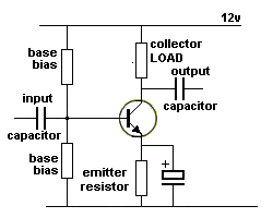
H-bridge circuit
The H-Bridge uses more components and requires more
current. It offers no benefit
and just requires more components and takes more current.
The only point I will cover is the input impedance. The base-bias
resistors "bleed" 10 times more current than the current required by the
base. The instructors on YouTube say this creates stability. But
that is not so. The circuit has a very low input impedance and it
attenuates the input signal by as much as 90%. This means the input
signal has to be 10 times larger than that required by the self-biased
stage to get the same results.
The self-biased stage is 10 times more sensitive and is classified as a
pre-amplifier stage. The H-Bridge is just an amplifying stage.
The two stages have completely different qualities and capabilities.
However they amplify the signal in identical ways and get the exact same
result. All the hype and false discussion surrounding one circuit
applies to the other.
In fact the self-biased stage employs negative feedback and this has
some impact on the quality of the amplified signal.
The
self-biased stage:
It uses 2 resistors, called the base bias resistor and collector load
resistor: This circuit will work from 3v to more than 9v.
The self-biased stage seems to have an overall gain of 70, no matter
what the gain of the transistor, due to the input current capability of
the signals we are delivering.
The value of the resistors are chosen so the collector is about half rail
voltage. This allows the transistor to deliver a signal
nearly equal to the value of the rail voltage to the following stage.
The value of the input and output capacitors depend on the frequency you are amplifying
and the values of 22n for the input capacitor and 100n for the output
capacitor are good for experimenting at audio frequencies.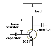
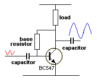
Self-biased stage
We are not going to use any mathematics or equations. But we are going
to give suitable values so you can experiment.
A small-signal amplifier stage has a load current from 0.1mA to 1mA -
NOT 10mA
A small-signal amplifier stage has a gain of 50 to 70. NOT 10.
The stage is called an AC STAGE or AC amplifier as the input and output
have capacitors so the stage is not affected by any other voltages. It
is separate and isolated from the voltages on the previous and next
stage. It generates its own set of voltages.
With the values we have chosen, the stage will produce a gain of 70 and
this means the amplitude of the signal will increase 70 times with an
input signal of 20mV.
The output signal will be about 1400mV when the stage is connected to a
following stage with medium impedance.
The stage we are designing will operate on a supply of 3v to 12v and
generally have a load current of 0.1mA to 1mA. With higher currents you
can get background noise.
This noise is generated in the resistors and the transistor and if a
high current is passed in an electret microphone the noise is like bacon
and eggs being cooked. A higher current is wasteful and shows you
don't know how to design a stage.
You cannot work out the gain of the stage with any formulae or
mathematics. You just
have to accept this value from the many experiments we have conducted
and the hundreds of modules and circuits we have made and sold: (over
300,000).
Sitting down with pen and paper and mathematics show your complete lack
of understanding of electronics. Transistors have enormous gain
variations and can operate completely differently than expected. They
have hidden zener features and current limitations and power
dissipations and losses, you never expect.
The self-biased stage is actually the stage we are referring to.
It has a base-bias resistor of about 1M or
more and it puts almost no load on the incoming signal.
The H-Bridge can be designed with high biasing values but generally
puts a higher load on the previous stage.
Electret microphones, dynamic microphones, pick-up coils and some Light
Dependent Resistors deliver a very small current and that's why the
self-biased stage is used.
SELF-BIASED STAGE CHARACTERISTICS
The self-biased stage allows the transistor to
be turned on by a very small current from the bias resistor and this
allows you to increase and decrease the current via an input signal and
the resistance of the transistor changes in a very linear way to produce
a distortion-free stage.
You will learn the transistor is simply a variable resistor and it is
the transistor in combination with the collector resistor that produces
a varying voltage on the collector that is passed to the next stage.
When a rising input signal enters the base, the transistor amplifies this about 200 times and the collector voltage falls. The current through the base-bias resistor falls and it reduces the effect of the incoming signal. That's why the transistor does not get the full effect and the gain is not as high as expected.
When the input signal falls, the transistor is turned off and the collector voltage rises. But now the base-bias resistor supplies more current to the base to turn it ON and this works against what the signal is trying to do. The end result is a gain of 70.
The following diagram shows the input signal is falling and at the same time the output signal is larger but rising. They are "out of phase" with each other.
The following circuit shows an electret microphone connected to the input of the self-biased stage and the component values to get a gain of 70.
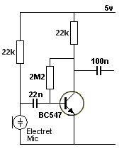
Component values and
Connecting an electret microphone
Matching the impedance of the electret microphone to the input of the
amplifier.
INPUT - OUTPUT CAPACITORS
This is something you cannot work out. You just
have to take my advice.
The LOAD for the microphone stage is 22k. The input of
the self-biased stage is about 3k to 5k as this is the effect of the
base-emitter junction.
You can see these two values are an enormous mismatch and that's why we
get the figure of 70 for the gain of the circuit.
The 22n also produces a considerable loss in the transfer of the signal
and you can get a CRO to see the losses.
When you see the signal on the electret is 20mV, this voltage is not
passed to the base of the transistor as a voltage. It is converted
into a current.
What happens is this: The electret turns off a small amount and the
voltage rises 20mV. This rise is passed through the coupling capacitor to the base of the transistor.
The current associated with this rise is passed to the base of the
transistor. The current is determined by the value of the load resistor
on the microphone. There is no way we know how much current is associated with
this rise as the capacitor is charging at the same time and removing
some of the energy. Whatever current is detected by the transistor is
amplified 200 times and some of the effect of this is delivered to
the output capacitor and to the next stage. But the output
capacitor and the next stage absorbs some of the energy that the
transistor is able to deliver and that's why, in the end, the result
we see is a gain of about 70.
The value of an output capacitor should be 10 times larger than the
input capacitor because the output will be handling a higher current and
the resistors around this part of the circuit will be much lower than
the value of resistors on the input.
2 FACTS
In the end, the value of the
input capacitor does not really matter, as long as it delivers the
amplitude. It can be higher than calculated and will not affect the
performance.
Secondly, the biasing of the stage does not really matter as the energy
entering the stage via the input capacitor will swamp the energy
provided by the biasing components. Suppose you have biased the stage so
the collector is at mid rail. It will require very little
current-reduction to turn the transistor OFF but a lot more
current-increase to turn the transistor ON fully.
How are you going to provide that requirement from a previous stage?
You can't !!
All this requirement about biasing a stage is completely redundant and
"falls over" when you see how a stage actually behaves when a signal is
processed. When a decreasing signal enters a stage, only the first part
of the signal turns the stage off and then the base becomes "open
circuit" and it does not remove and of the incoming energy. The
only energy that is removed is done by the biasing component and this
removes very little. The charge across the input capacitor hardly
changes.
That's why you should pay very little attention to the mathematics of
designing these stages, as the stage will create its own results and
they will be completely different to anything you have predicted.
THE LOAD-LINE
Let's go over the
hype of designing a circuit, again.
So much time is wasted on talking about the LOAD LINE for a
stage.
This is the concept of placing the transistor in a mid-bias state so the
positive and negative excursions of the input signal will be equally
amplified.
But let's go into the truth.
The transistor is sitting at mid-rail and the transistor is receiving
this "turn-ON" current from the biasing components.
But here's the point that no-one mentions.
It only takes a small current to get the transistor to "half-turn ON"
It takes a lot more current to turn ON fully.
An input signal has a lot of current-capability when it starts at zero,
and as the input signal rises, the current capability decreases.
This is because the input signal is generated from the LOAD RESISTOR of
the previous stage and as the voltage across this resistor decreases,
the current it can supply DECREASES.
The voltage across the resistor decreases, mainly because the
stage-coupling-capacitor charges.
So we have two conflicting situations.
The signal finds it very easy to start to turn the transistor ON and as
the signal rises, it has less energy to deliver this energy into the
base, while the base wants more and more energy to turn the transistor
on HARDER and HARDER.
In other words we have two situations that do not match each
other AT ALL.
The effect is this: When the signal starts to rise it has a very big
effect on turning the transistor ON and when the signal reaches its peak,
it has very little effect on turning the transistor ON.
So, the curve of the input signal is not reflected in the output of the
amplifier AT ALL.
That's why you can't do any mathematical calculation. You have no
parameters, no values, nothing to go-on.
Even if the inter-stage coupling capacitor does not charge and reduce
the transfer effect, the "turning-ON" of the transistor in the stage we
are designing takes more current for each percentage increase in the
"turning-ON process" and this is far from a linear relationship.
It's amazing the amplifier works at all, but because the whole thing is
so sloppy and so tolerant and so non-demanding, you get an output
signal that is recognisable.
Once you realise this, you will see how far off the mark the instructors
are. Things DO NOT MATTER. Just about any values will work and all you
have to do is listen to the output and adjust the values until you get a
clear reception.
Let's mention another point that has never been covered.
As the input signal rises, the input capacitor may or may not charge. As
long as the input signal is higher than the voltage on the base and
higher than the input lead of the capacitor, it has "headroom" and will
deliver current to the base. When the signal reduces, it also delivers
energy to the base. The base will only rise and fall a few millivolts,
and as soon as it falls below 550mV, the transistor does not accept any
more current.
This means the input signal only has to be 50mV in amplitude and if it
can supply current, the circuit will work perfectly.
That's why the amplitude of the input signal is quite unimportant. It is
the current-carrying ability of the signal that the transistor detects.
WHAT REALLY HAPPENS TO THE INPUT
SIGNAL
The diagram shows a transistor with a resistor
connected between the collector and the 12v rail. The resistor is called
the LOAD.
This will make the transistor turn on "more and more"
and its effective resistance will be less and less. This means
more and more current will flow through the LOAD resistor.
3 simple questions:
2. If the base-bias resistor in a self-biased stage is
increased, what will happen to the collector voltage?
0.7v BASE VOLTAGE
A SURPRISE!
Page1A. more on the stages
Contact Colin
Mitchell if you want any help Go to
Talking Electronics
website
9/9/2023
The input signal to a transistor stage might be 1mV in
amplitude or several volts.
Once a transistor is "turned on" via the components in a stage, the base
does not want or need an increased voltage. It just need an increased
CURRENT.
So, what happens to the 1v input signal?
The input signal has a current-capability associated with it. This is a
difficult fact to understand, but for the moment we will just say that
all input signals have a current capability. If the current-capability
is very small, the 1v signal will not be amplified very much. If it has
a lot of current capability, the 1v signal will be amplified the
greatest amount.
I am not going into the amount of current needed, but the signal will be
able to deliver a higher current into the base of the transistor when
the input signal is a maximum.
The transistor does not know the voltage of the signal but it detects
the increased CURRENT. In other words, the amplitude (voltage) of
the input signal is converted to an increased CURRENT and the transistor
will amplify this current 100 to 200 times.
The voltage on the base may increase a small amount but we do not know
how much, and this increase NEVER comes into any calculation.
So, the VOLTAGE is CONVERTED to CURRENT.
The signal is like a car battery. The battery might be capable of
supplying 400 amps, but a car globe will only consume 10 amps.
The same with an input signal, it might be capable of delivering 100mA,
but the transistor will only "ask for" (require) 2mA.
But if the signal can only supply 2mA, its voltage will drop by about
50%. The theory behind this is a whole new discussion.
That's why it is important to know the current-capability of the input
signal, so that it is not reduced by the transistor stage.
And that's why it is important to have a high impedance input for the
transistor stage, so little or no attenuation is produced.
You cannot find and you cannot work out the impedance of a transistor
amplifier because it will vary according to the surrounding components
and the current entering the base.
The highest input impedance applies to the self-biased stage while the
H-Bridge design has the input reduced by up to 90% due to the bridging
components. This means the effectiveness of the input signal reduces to
10% and the stage has to amplify the current 10 times just to regain is
effectiveness.
This means the amplitude of the input signal REDUCES TO ZERO AT THE
BASE and only the varying current enters the transistor.
Now you know why all the text books, University lectures, and YouTube
videos are so inaccurate, misleading and uninformed.
This is the most important factor to understand with transistor
circuits.
All the diagrams show voltage amplification, but the transistors only
see CURRENT VARIATIONS.
If you could inject the base with a voltage having NO amplitude; but a
varying current, it would work exactly the same.
But it is the voltage that allows the current to increase and this is
what the transistor wants.
HOW DOES A TRANSISTOR WORK?
I have seen so many complex discussions on how a transistor works, that no
beginner will understand how it actually works, when the explanation is
so complex.
So, here are the simple facts:![]()
The base is the input and the collector is the output. The
emitter just keeps the transistor "in place."
The transistor is just a variable resistor. That's all it is.
Just a variable resistor.
When nothing is connected to the base, the transistor has a very high
resistance. We mean it has a very high resistance between the
collector-emitter terminals.
When you connect a voltage to the base, the resistance of the transistor
decreases.
But it is not just the voltage that the transistor sees. It sees the
current you are supplying.
You can supply the transistor with a small current by adding a "safety
resistor" to the input voltage and as you reduce the value of this
resistor, the current into the base will increase.
![]()
Supplying a small current to the base
All transistors have an AMPLIFICATION FACTOR called GAIN and it is
normally greater than 100. This means the current supplied to the base
will be increased 100 times through the LOAD.
We are not going into any mathematics but the voltage on the collector
will rise and fall when the base current decreases and increases and
this is how a signal is amplified by the transistor.
A signal has a certain amplitude and a certain "strength."
Its "strength" is the amount of current it can deliver. But a
transistor does not "deliver" a current. It simply reduces
resistance between the collector-emitter terminals and this allows more
current to flow through the LOAD. As a signal
moves through each stage of amplification, it increases in amplitude and
also increases in "strength."
The transistor is just a variable resistor. It is the surrounding
components that create the increase in amplitude and strength of the
signal.
We say this to keep the discussion simple.
Later you will learn how the surrounding components create the amplitude
and strength of the signal.
At the moment you just need to understand the CURRENT into the base
decreases the resistance of the transistor. The transistor is a CURRENT
controlled device. There are other types of "transistors" that are
voltage controlled (FETs).
But the transistor (shown above) does not increase the current. It
allows a higher current to flow through the LOAD. This is because its
resistance decreases and a higher voltage will appear across the load
and thus more current will flow through the LOAD.
This current also passes through the transistor. It is the LOAD that
"asks-for" or "demands" the extra current and the
transistor allows the current to flow.
It is the LOAD that does all the "demanding." The transistor simply does its job and
allows the current to flow.
You have got to understand, the transistor "sits back" and does very
little of the "decision-work" It is merely a variable resistor and
the surrounding components create all the voltages and gain and even the
quality of the signal.
That's why everything you have been told in any lecture and text book
has "side-stepped" the real way things work and that's why you have
little understanding of how to design things.
It's like them telling you SANTA is real. You are living in a
total miss-conception.
1. If the transistor in a self-biasing stage is replaced with one having
higher gain, what will happen to the collector voltage???
3. What is the ratio of input to output capacitor values?
As you can see, the
real way the circuit works is completely different to anything that has
been explained in any text book. Unless you know how a circuit works,
you cannot find and fix a problem.
Answers:
1. The collector voltage
will fall. 2. The collector voltage will rise 3.
Output capacitor is 10 times larger.
There are so many
misconceptions and false discussions about the base voltage being 0.7v.
Firstly you cannot deliver 0.7v to the base and expect the transistor to
work.
Secondly you cannot provide ANY voltage to the base. You have to provide
a higher voltage via a current limiting resistor and allow the
transistor to create its own voltage on the base.
And thirdly, you have to place the transistor in a circuit so the
transistor and surrounding components all the transistor to produce the
EXACT voltage it needs.
In other words, you should do very little or PRACTICALLY NOTHING about
setting the base-emitter voltage.
In fact, the operation of the transistor has NOTHING to do with the
base-emitter voltage.
The base-emitter voltage is VERY critical and one transistor may have
635mV on the base when it is quiescent mode (idle mode) and and it rises
to 645mV when operating. You might think this is a small rise, but the
rise have nothing to do with the current-capability of the transistor.
The current may be 0.1mA when the base-emitter is 635mV and rises to
645mV when 10mA flows. This is less than 1% rise in voltage but
the current increases 100 times !!
The operation of a transistor is completely NON-LINEAR and I have never
mentioned the base-emitter voltage in any of my discussions because it
has absolutely no bearing on designing a circuit.
As long as the transistor gets its "turn-on" voltage, the transistor and
surrounding components will do the rest.
All the discussions that add 0.7v or take off 0.7v, is like me saying I
gamble $3,500.32 each day.
THE TRUTH
Now we come to the truth.
You cannot design a circuit without knowing the characteristics of the
stage before and after the self-biased stage you are designing.
All the instructors on YouTube don't have a clue about designing a
stage. They have never designed a circuit in their life.
The effectiveness of an input signal depends on its CURRENT-CAPABILITY.
In other words, the IMPEDANCE of the signal - the strength of the signal
being supplied by the electret microphone stage.
You will notice the electret microphone does not "drive" the signal into
the self-biased stage, but the microphone turns OFF and the current IT
DOES NOT TAKE is passed to the stage via the LOAD resistor, through the capacitor
to the base we are designing.
It's a bit like you earning $1,000 a week and you spend as much as you
want and the odd change at the end of the week is given to your family
to buy food. They won't get much. And the amplifier does get
much either. It only gets a 20mV rise via a 22k resistor. This energy
passes through a capacitor that absorbs 30% (as it gets charged during
this time). There is very little left for the transistor amplifier.
The incoming signal sees the base of the transistor as a 5k
resistor (resistance - impedance).
In simple terms the 22k becomes 40k (due to the losses incurred by the capacitor) and now it is
passed into 5k. This becomes an enormous voltage mismatch and that's why
we can only deal with it as an "energy package."
But if the 22k load resistor was 1k, a lot more energy would be
transferred. That's why you really cannot make any calculation because
you don't know the real impedance of the base-emitter junction and you
don't know how much energy it gets.
The same applies with the output.
If the stage (following the one we are designing), is removed, the amplitude of the signal on the
collector of the self-biased transistor may be as high as 2,000mV. But
when the following stage is connected, it will drop to 1,400mV or even
lower.
This is because the base-emitter junction of the following stage and the
effect of the output capacitor create a voltage-divider with the collector load
resistor.
So, the gain of the stage we are designing depends on the input
impedance of the stage that follows.
We can increase the gain by reducing the value of the load resistor on
the collector and reducing the value of the base-bias resistor so
the stage sits at half-rail voltage but it draws a higher current.
Or we can
reduce the impedance of the input of the stage that follows.
But this is only half the
story. You cannot start to design a stage until you know: "what
you are driving into." You need to know the input
impedance of the stage that will follow.
That's why none of the videos on the web have any value.
They are just a JUNK presentation.
How do you think I can see a circuit working "in my head" and solve
problems and design things without any paperwork?
Because I see how a transistor REALLY WORKS. It works completely
differently to anything you have read or viewed and anything we have
covered above.
If you really want to know how a transistor works, FORGET EVERYTHING you
learnt.
A transistor is just a variable resistor. It does NOT produce the output
waveform. It does not produce the gain or the size of the signal.
All it does is allow a current to flow in the collector-emitter circuit.
It does not have anything to do with voltage . . .. it does not control
the voltage.
The item that produces the output waveform is the LOAD RESISTOR and you
are going to learn one of the most important concepts of electronics,
that has NEVER been discussed.
It is called CONVERSION.
And it all revolves around 2 resistors IN SERIES that create a VOLTAGE
DIVIDER.
A Voltage Divider consists of 2 resistors in series and when they are
equal, the voltage at the join is half the supply voltage.
If you decrease the value of the lower resistor, the voltage at the join
decreases.
There is one more concept you have to understand. If you connect
something to the join, you will mess up the voltage and that's why we
are going to assume you do not connect anything. The transistor is the
lower resistor. When you don't supply any current to the base of the
transistor is has a very high resistance.
This means the join of the two resistors will be very close to rail
voltage.
When you supply a lot of current to the base, the transistor will have a
very low resistance and the join will be very close to the 0v rail.
That's how the output signal rises and falls.
We supply CURRENT to the circuit and the LOAD RESISTOR converts this to
a rise and falling voltage output.
I never mentioned the input VOLTAGE. I don't need it.
So, a varying input CURRENT produces a varying output VOLTAGE. This is
called CONVERSION.
The transistor cannot do this without a LOAD RESISTOR.
But in a practical circuit the output signal is passed to the next
stage, and the next stage wants CURRENT to do the same thing as the
stage we have described.
Each stage in a circuit normally wants 10 to 100 times more CURRENT than
the previous.
This is called "Bleed-off" and upsets our discussion about voltage at
the mid-point.
So far we have a lower resistor can can go from a low to high value and
change the voltage at the midpoint from a low value to a high value. But
the next stage is like putting a resistor from the mid-point to the 0v
rail.
You have to learn about a voltage divider with a fixed resistor.
Suppose the load is 10k and the resistor on the output is 10. These two
create a voltage divider in which the voltage at the join is half-rail
voltage.
This means the transistor can only reduce the voltage to 0v and the
signal is immediately less than half the expected.
Use the same reasoning to see the voltage will never rise as high as
before.
This is what I see when I look at a circuit. I see voltage dividers and
the results have nothing to do with the voltage-amplitude of the input
signal, the gain of the transistor or the output current of a stage.
With this simplified approach you will be able to mentally diagnose a
stage to 90% success and only an examination of the stage "in action"
will get a closer result.
All the mathematics you have been lumbered with "flies out the door"
when you understand how the stage really works and you can see why a
University could not charge $19,000 for our way to do things. Not only
would they produce a capable, competent student, but show up the text
books for their worthlessness.
Page-2 emitter-follower - common collector stage
Page-2A common base stage
Page 3 Coupling stages
Page 4 More on Coupling Stages
Page-5 The FLIP FLOP
Page-6 All the "YouTube" mistakes
and the Common Base Circuit
The transistor Potentiometer
The
REAL
Transistor Amplifier