|
The |
Which
circuit do you use? What is the difference? Which circuit is
the best?
There is no rule to follow but when you understand the different
features and characteristics of each stage, you can make an informed decision.
The first circuit is called a SELF BIASED STAGE. The
second circuit is called a H-BRIDGE arrangement. 
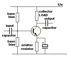
Basically the first circuit has a large input impedance and will
amplify very small, weak input signals and produce a stage gain of about
70. This value is nearly always the same when the correct component
values are used. This is what we call a pre-amplifier stage.
The second circuit is called an H-BRIDGE and can amplify a
stronger input signal and produce a stronger output signal. The gain of
the stage can be set to 2 or as high as about 100. The
things that make the input impedance lower than the first circuit are
the base bias resistors. They are designed to make the stage "stable"
and produce the same gain over a wide range of supply voltages and
temperatures, but they have an attenuating (reducing) effect on the
signal.
One of the biggest myths is the current through the
base-bias resistors of an
H-BRIDGE circuit must be 10 times the base current.
If the base-bias
resistors are passing 10 times the base current, this means you are
fighting against resistors that will remove up to 90% of the energy of
the input signal.
What an absurd design . . . if you are trying to amplify a very
small signal!!
They use this rule because they think the resistors are VOLTAGE DIVIDERS as in a
voltage dividing circuit where the bleed resistors take a high current
to stabilize the output voltage.
But in this case the resistors are a voltage divider for the quiescent
conditions of the circuit and when an input signal is applied, the
base-resistors can actually be removed!!!
Further to this they say the resistors make the circuit stable as far as
gain is concerned and it does not alter with transistors of different
gains.
But the emitter resistor and emitter-bypass electrolytic has an effect on the gain of the
circuit and as the frequency increases, its value decreases and this
increases the gain of the circuit.
On top of this, the emitter by-pass capacitor is such a high value that
it does not have any time to charge and discharge during a cycle and so
the emitter is essentially FIXED IN PLACE and thus the transistor
operates with the maximum gain the transistor can provide.
This is generally an unknown value and it is pointless producing calculations to
deliver values accurate to 0.1%!
The emitter resistor is called an EMITTER FEEDBACK RESISTOR and
it has an enormous effect on stabilising the "rest conditions."
You will learn the designing of this is stage is done "backwards" and
you work from the output to the input. This approach has never been
covered because none of the instructors have ever designed a circuit in
their life.
That's why all the text books and lecturers are just following what they
have read, without "looking outside the box" and seeing if the
information is accurate.
As I said, there are no rules, but the first circuit is ideal for
amplifying signals from less than 1mV to say 20mV (or slightly higher) and
having a current capability of a few microamp to 1mA.
The second circuit can be used with a signal from 1mV to say 100mV and a
current capability of 1mA to 10mA. This is just a guide.
In all the cases of "gain" we are talking about voltage amplification.
The current will also increase and so the circuit is doing two things at
the same time.
All these circuits are very hard to understand because we talk about
voltage increase and signal amplitudes but the circuit is really using
the current associated with the signal to produce the level of
amplification.
And secondly, the transistor is not producing the larger signal or the
increase in current.
It is allowing the LOAD resistor to do both of these functions.
The transistor is merely a variable resistor and the increased current
comes from the LOAD (because the LOAD is connected to the supply rail .
. . .
where the current "comes from.")
That's why all the YouTube videos and text books are omitting the REAL
details of how the circuit works and when you design a circuit that does
not work, you will be unable to diagnose it. That's why you have to know
the finer details.
You cannot fully design a transistor stage without knowing the characteristics of the input signal and the value of the stage that you are sending the signal. You see stages designed on YouTube without any reference to the input signal or what the circuit is passing the signal to. .
That's why all those videos are worthless.
Not only do you need the characteristics of the input signal but you also need the characteristics of the next stage in the amplifier.
If the input signal is "weak," the stage you are designing will attenuate the signal considerably and you will be disappointed.
In all case the input signal is reduced when it is connected to the input of a stage because the stage is using some of the energy of the signal to operate the transistor.
In other words you can see the amplitude of the signal you are supplying on a CRO when it is not connected and then connect it and the height of the signal will be reduced.
It is taking away the "current" part of the signal but since we cannot measure this (current) effect, we have to accept a visual effect and that is the voltage waveform.
The same applies when the stage you have designed is connected to the next stage.
The amplitude of the signal on the collector (of the stage you have designed) will be reduced considerably when the next stage is connected.
That's because the next stage is using some of the energy of the signal to operate the transistor.
THE INPUT AND OUTPUT
CAPACITOR
HOW DOES THE SELF BIASED STAGE WORK?
The transistor is turned ON with about half a microamp via the 2M2 and
the circuit is classified as "High Impedance." You will only be able to
measure the voltages with a digital multimeter and NOT an analogue
meter, as you don't want to upset the circuit.
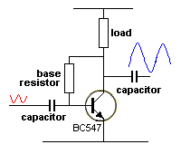
Before we go any further, I will include a circuit from YouTube. It
shows a BC547 driving an 8R speaker.
The input and output capacitor (and inter-stage coupling capacitor)
works in two different ways, depending on its value.
If the value of the capacitor is small. it will charge and discharge
during each cycle and some of the amplitude will be lost when it does
this.
But if the value is "extra-large" it will not charge or discharge but
one of the leads will rise and fall and the other lead will rise and
fall, exactly the same amount. The circuit will think it is connected directly to the other lead.
If a lead connected to the base of a transistor will not rise above 0.7v
but the "pulling effect" of the rising input signal will appear to act
directly on the base. It will be the "pulling current" that transfers
the energy.
In this case you do not have to worry about the "effective resistance"
(capacitive reactance) of the capacitor.
When the value of the capacitor matches the resistance of the components
on the output, it can increase the amplitude of the waveform and we have
covered this in these pages. This applies to some of the push-pull
circuits and emitter-follower circuits.
When a capacitor is connected to the base of a transistor, the base cannot rise above 0.7v
and if it goes below 0.55v the transistor turns off. So, you only have a very small voltage range from 0.55v to 0.7v and
if you measure this voltage accurately it will tell you the amount the transistor is "turned ON" or
being "pulled-ON."
The voltage range is very small but the current range can be from 0.01mA to more than 50mA for
the base of a small-signal transistor and when this current is multiplied 100 times,
by the amplifying effect produced by the transistor, the collector
current will be very impressive. It is the CURRENT being transferred
that delivers the "signal" from one stage to the other. It is the effect
of the voltage divider, made up of the load resistor and the transistor
that produces the signal amplitude or signal increase or waveform
increase. You have always got to remember the transistor is just a
variable resistor.
We are going to study the
SELF BIASED STAGE as it is ideal for amplifying very small
signals. A very small signal can be as small as 1mV and have a
current capability of ONE MICROAMP. Here is the
SELF BIASED STAGE:
How does a 1mV signal drive a stage?
The secret is this: The stage is already turned ON and the transistor is
accepting exactly the right amount of current into the base. You cannot
do this yourself but the base resistor does this automatically, due to
the way it is connected in the circuit.
The amplitude of a weak input signal might be reduced by 50% but the
circuit is really using the current part of the signal . . . . so why talk about
the voltage!!!
The fact is this circuit is the ONLY circuit for tiny signals and will
even pick up "hum" from the surrounding when you place a finger on the
input.
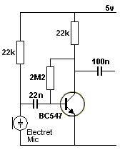
By connecting 3 transistors as shown in the following circuit, you can create an input so sensitive that it
will pick up "ghosts:"
The values of 2M2 and 22k have been used (after experimenting with
the circuit and selecting the base-bias resistor) to produce half-rail
voltage on the collector. We want the LOAD to be 22k so the circuit
will take less than 1/10th of a milliamp from a 3v battery and it
will be active 24 hours a day as a listening-device. So, we start with
22k LOAD.
How does the circuit self-adjust?

Suppose we deliver a 20mV waveform with a current capability of 1
microamp.
The base is already getting about half a microamp and when we deliver
another 1 microamp, the transistor will turn ON and the collector
voltage will fall to about 0.8v. The voltage across the 2M2 will be less
and thus the current flowing through it will reduce. It will only
deliver one quarter of a microamp.
This means the transistor will not see 1 microamp but about 0.75
microamp. Thus some of the effectiveness of the signal has been lost.
When the voltage of the input signal moves in the opposite direction, it
will remove 1 microamp from the base-bias resistor and the transistor
will turn OFF.
The collector voltage will rise and now the 2M2 has a higher voltage
across it and it will deliver about 1.2 microamp. This will cancel
the 1 microamp from the signal and the transistor will be turned on a
small amount.
The peaks and lows of the input signal will be reduced as well as the
transistor will want more current from the signal and that's why the
circuit produces a gain of about 70, after all the losses have been
taken into account.
If we use a transistor with a gain of 250, why do we get a gain of
about 70 from the circuit?
The transistor uses the CURRENT value (the value is milliamps or
microamps) of the signal. .
The transistor is already "turned-ON" via the base resistor and if you
deliver a signal to the amplifier via the input capacitor, it will have a
very small current and the transistor will amplify this current by
turning ON more and allowing an increased current to flow through the
LOAD resistor. The transistor becomes a smaller resistor and it combines
with the LOAD resistor to create a new value of resistance. This new
value allows a higher current to flow and the voltage at the join
reduces.
This circuit does not and will not work because the speaker has a very
low resistance and the collector current will be greater than 100mA and
the transistor will be damaged. The collector current must always be a
lot less than the maximum specified, to prevent overheating.
On top of this, the stage will fail to work with a higher-current
transistor because the gain of a transistor reduces enormously when the
current is near the maximum allowable and the 10k will not turn ON the
transistor to produce mid-rail operation.

OF AN INPUT SIGNAL?.
You really don't need to determine the suitability of an input signal as
the circuit we are discussing is the most sensitive you can create and
if you want to look at the signal on the collector of the transistor,
you can buy a very low cost digital CRO, with storage and "viewing
capabilities, for $50.00:


It's all you need for audio circuits and once you get to know how to
operate the features, you can see the signal at each stage of
amplification.
Here are some circuit values for supply rails from 3v to 6v:

For 9v to 12v, simply double each of the values.
When we specify a BC547 transistor we are indicating the transistor has no
special features and almost any small-signal transistor can be used.
No mathematical calculations are needed.
All you need to do is measure the voltage on the collector of the first
transistor and see if it is about half-rail voltage.
If it is higher than half-rail, decrease the 2M2 to 1M8 or 1M5. If the
voltage is higher than half-rail, use a 3M3 resistor.
The first circuit above has two stages. The first stage is the electret
microphone and 22k LOAD resistor. The second stage is the transistor
amplifier. Our test circuit produced a gain of 35 when the load was
reduced to 10k on a 6v supply.
For the second circuit, select an emitter resistor to produce about 1v
across the electrolytic.
COUPLING CAPACITOR
What happens when you use a very large coupling capacitor?
Basically the circuit will still work but with reduced transfer of
energy from one stage to the other.
A coupling capacitor only transfers the maximum amount of energy
(signal) when it is discharged fully during each cycle.
It is only the CHARGING CURRENT that one stage transfers to the next.
If the capacitor has not fully discharged, only a small amount of energy
will be transferred. If the capacitor is fully charged or even partially
charged, the LOAD resistor cannot deliver any current to the following
stage. The capacitor merely delivers a voltage to the base of the next
stage that is below the turn-on voltage for the base and up to nearly
the turn-on voltage and maybe deliver a very small amount of energy.
That's why you get distortion.
The time taken for a capacitor to fully charge is called the "time
constant." And one-time-constant is the time taken to reach 63%.
Full charge takes 5 time-constants.
The length of time depends on the value the capacitor and the resistor
connected to it (in series).
For example
100n and 10k takes 1mS for one-time-constant. If you
have a 1kHz signal, it takes 1mS for 1 cycle.
This is only half-millisecond for the rise time so the signal has to be
500Hz for the capacitor to have to time to reach 63%.
If you have 1u and 10k, one-time-constant is 1/100th of a second. So the
frequency has to be 50Hz for one-time-constant to apply.
But we are considering the DISCHARGE time for the capacitor.
This means, as you increase the frequency, one-time-constant
discharges the capacitor to 33% of its original charge.
So, you can see, we are not talking about the reactance of the capacitor
(its effective resistance) but its effectiveness in transferring energy
from one stage to the next.
It's very easy to CHARGE a capacitor, but no-one looks at the
DISCHARGE.
For example, in the following circuit there is NO discharge path:

If the left lead of the capacitor drops 1v, the right lead drops 1v too.
During this time, the base will accept current from its initial value of
0.7v, down to a value of 0.55v and at this point the base-emitter
junction does not accept any current. Remember, he base can never rise
above 0.7v.
So, we have discharged the capacitor during only 0.15v of its excursion, but
we don't know how much of the charge has been passed to the transistor. Certainly not
very much. It is only this amount of energy that can be transferred
during the next half-cycle.
That's why capacitors are very inefficient in transferring energy.
No-one has pointed out this fact.
They only take into account the effective "resistance" of the capacitor
at a particular frequency. This is only a fraction of the information
you need to know.
DESIGNING AN H-BRIDGE CIRCUIT

The H-BRIDGE circuit is designed from
the output to the input as this is the only way you can do it.
The only thing you need to know it the resistance (impedance) of the
load you are driving.
Obviously we want the larges amplitude to be delivered without
distortion.
If we have a 100R load, we can deliver a maximum HIGH of 3.7v as the
output become a voltage divider when the transistor is turned OFF and
the 220R and 100R become a voltage divider with the output in the
middle. We assume the 10u will not charge during this time and will not
discharge during the second part of the cycle.
The current flowing through the voltage divider will be 12/320 =37mA
When the transistor turns ON, it will pull the 10u down and we have to
find out the minimum output voltage for this part of the cycle and also
the current through the 220R.
Determining this value is a little tricky.
When in the quiescent (resting) state, we want the current to be about
2mA.
This means the voltage across the 1k emitter resistor will be 200mV and
the voltage across the transistor will be about 0.3v, when it is fully
turned ON, so the minimum voltage will be about 0.5v.
This means the voltage across the load will be 3.2v
The quiescent current through the transistor will not affect the value
of the output amplitude very much because the transistor will be turned
ON and OFF by the incoming signal and the best you can expect is 3.2v
If 200mV is developed across the 1k, only about 40mV will appear across
the 220R. So the transistor will be turned ON a very small amount.
You don't know if the transistor has a gain of 100 or 250, and you can't
guess the value of the base resistors. It is pointless calculating their
value as the fastest way to get the correct values is to build the
circuit. Don't even bother to learn the mathematical expressions as you
simply leave the ID on the Printed Circuit board as "A" and "B"
and provide the values when assembling.
MEASURING CURRENT
It is
difficult and awkward to measure current through a component and you can
use this simple way to obtain the value.
Measure the voltage across a component and by Ohm's Law, you can obtain
the current.
If you have 10v across a 10k resistor, the current will be 1mA.
If the voltage is 1v across a 1k resistor, the current will be 1mA.
If the voltage is 1v across a 100R resistor, the current will be 10mA.
If the voltage is 1v across a 1R resistor, the current will be 1 amp.
If the voltage is fluctuating, use an analogue meter to see the needle
flutter.
You do all the CURRENT CALCULATIONS in your head.
You start with the basic Ohm's LAW: One volt appears across
one ohm when 1 amp is flowing.
You simply divide one value by 100 and multiply the other by 100.
One volt appears across 100 ohms when 10mA is flowing.
One volt appears across 1k ohms when 1mA is flowing.
HOW to "see" A CIRCUIT WORKING:
Take the following circuit
above for example.
We have to know some things and we assume the signal generated by the
electret microphone is 20mV. The microphone LOAD resistor is 22k and
this is the resistor generating the current for the transistor
amplifier.
The LOAD for the transistor is 22k so we can directly amplify the 20mV
by our accepted gain for the stage to get 20 x 70 = 1400mV = 1.4v
That's about as much as we can assume.
The next circuit comes from YouTube

The mistakes involve concepts you have not been taught.
Basically the mistakes revolve around the 2 diodes and the 10k
resistors.
When the voltage on the 100u input capacitor rises, the action is
designed to turn on the top transistor as an emitter-follower.
But the diode is stopping the 100u having any strong effect on raising
the top transistor.
The diode will just "turn-around" and sit as shown in the diagram below
and no matter how high the 100u rises, the voltage will simply be
developed across the diode and the 100u will have no effect on driving
the load.
The only component that will raise the top transistor is the 10k base
resistor.
Here's another circuit feature you need to know.
The transistor will convert the 10k into a low-value resistor and the
transistor can be replaced with it. The value is 10k divided by the gain
of the transistor. If we assume the gain is 100, the new value is
10,000/100 = 100 ohms.
The output 100u is being pulled up by a 100 ohm resistor and the load is
50 ohms.
If we assume the 100u has no voltage across it, the LOAD will see 50/150
= 0.3 x 10v = 3.3volts.
But the "pulling power" of the 10k (100R) DECREASES as the emitter of
the top transistor rises. At the mid-point of its travel, the 100R has
only half the "pulling power" and almost no "pull" at the top of it
travel. The "pulling power" depends on the voltage across it and the
voltage across it allows current to flow into the base of the top
transistor and this allows the transistor to pull the emitter "UP." So
the 3.3v stated above will actually be less.
We can find the approx voltage across the 100u from the "time constant"
information described above.
If we assume a frequency of 1kHz, it will take about 1mS to charge to
63%, so the real voltage is be less than 2 volts.
This is a lot less than the expectations of a properly-designed circuit.

All you have to do is connect the 100u input electrolytic to the two
bases of the transistors and the electro will have a strong effect on
driving the output transistors.
But this depends on the input signal having the "pulling power" make the
input 100u rise. In other words the input signal has to be LOW
IMPEDANCE.
That's why you have to be aware of how to connect components to avoid
circuit
mistakes.
The following circuit shows how to connect the 100u:

Here is another disaster from YouTube:
It is full of mistakes.

The base bias resistors are the wrong values. Work out the problem in
your head. Suppose the base resistors are 500k and the voltage is 10v.
This puts 2v across each 100k. The 10k will have 0.2v. This is not
enough to turn ON the transistor.
When the transistor turned OFF, the 2k resistor will be in series with
the 8R speaker.
If the supply is 10v, the voltage across the speaker will be 1/20th of
the voltage across the 2k. 1/20th of 10v is 0.5v. In other word
the speaker can see a maximum of 5%.
That's how you look at a circuit and instantly see it will not work.
The next example is GOOD design.

It is designed to amplify the audio from your mobile phone.
The base resistors put about 1v on the base and this produces about 0.4v
across the 22R.
About 2v will appear across the 100R, giving about mid-rail voltage for
the collector when in
rest state.
The 100R will be able to pull the 10u output electro UP and the
transistor will be able to pull it down via the 22R.
This is one of the best designs for delivering a signal to an output
such as 16R or 32R earpieces.
Here's another poor example on YouTube:

The base bias resistors are designed to keep the transistor OFF but the
low value of 500R in combination with the 10k input signal will deliver
500/10,000 = 5% of the input signal to the base. This is a
reduction of 20 times. And you need a gain of 20 to overcome this loss.
We don't know the current capability of the input signal or its
amplitude but getting only 5% will deliver a lot less than expected.
We cannot do any more analysis without knowing the value of the
capacitors.
There is so much false, misleading, inaccurate, information on the web,
including lectures from Universities, that I understand why the student
emerges with a worthless piece of paper at the end of 5 years.
I have never found a lecture that is "spot on" and explains what the
topic is trying to achieve with an explanation that is simple to
understand.
At the end of the video I ask: "What does the circuit do?" "How
can I interface the circuit?"
"How can I look at the circuit and work out component values without
using any mathematics?"
None of these things are answered or even contemplated.
No-where, ever, has any lecturer ever discussed fault-finding a circuit.
And yet this is one of the challenges you will be involved in every day.
Circuits don't always work the first time and most of the time you want
to improve the performance. None of this has ever been covered.
The designer of the following circuit made one mistake:

The collector resistor is 10k. When the transistor turns OFF, the
10k will pull the 10u output capacitor HIGH. The 10k will form a voltage
divider with the impedance of the earpiece inserted in the jack.
Suppose the impedance is 64 ohms, (to allow for the highest impedance
possible).
The earpiece is going to get a percentage according to: 64/10,000 and
this is less than 1%.
That's why I promote my "visual" way of seeing how a circuit works.
I have already stated that the transistor does not deliver any signal to
the output. All the does is TURN OFF and the load resistor does all the
work.
When you understand this, you will not make a mistake as above.
The transistor "pulls down" to deliver the negative half-cycle but the
load resistor provides the other half.
NPN AMPLIFIER

Designers think they can put any value component on the output of a
stage and it will deliver a waveform.
This circuit is no different to an NPN stage. The 100u is pulled UP by
the transistor and approx 6v will appear across the 1k LOAD.
But the circuit has one major mistake. Since the output capacitor
is so large, it will take time to charge and discharge.
It takes about 1/4th of a second to charge so any frequency above 10Hz
or 100 Hz is going to prevent the capacitor charging. Suppose the
capacitor charges to 12v (which it will never do) and the transistor
turns OFF. The 12v on the capacitor will be like a 12v battery and
the circuit will be 5.1k and 1k. The 12v will be across 6.1k and the
voltage across the 1k will be 6/12 = 2v. So the capacitor does not
operate in this mode.
It operates in an UNCHARGED MODE. Or a microscopically-charged mode.
The transistor turns ON and delivers 6v signal to the load and it pulls
up with a impedance of 1.2k .
When the transistor turns OFF, the load sees zero volts.
Why do you have to learn about the transistor?
You need to learn how a transistor works because it is still needed in a number of circuits to connect an outside device to say a module or microcontroller.
The effectiveness of a transistor is also represented in an IR receiving transistor.
However there are hundreds of circuits that use a transistor and need a lot of skill to understand the impedance implications and none of these circuits have ever been discussed in any text book or lecture.
You will see a lot of these circuits on Talking Electronics website, in projects and modules, but the operation of the is not discussed as they are ready-built modules for Model Railway projects.
Unless you cover these circuit you are only 1% informed and don't have an understanding of interfacing.
Courses are totally inadequate as far as education is concerned and going by the incompetence of the instructors to describe how simple amplifiers work, they would have "Buckley's chance" of interfacing to a module.
None of them have discussed IMPEDANCE MATCHING in a way I understand what they are trying to get across and the student would have less than zero chance of understanding the concept.
All circuits work on VOLTAGE DIVISION and IMPEDANCE MATCHING.
A transistor is just a variable resistor and it does not produce voltage amplification. It is the surrounding components that do all the work.
That's why you have to totally disconnect from anything you have learned, to really and fully understand how to design circuits.
Page-1 Common-Emitter stage
Page-2 emitter-follower - common collector stage
Page 3 Coupling stages
Page 4 More on Coupling Stages
Page-5 The FLIP FLOP
Page-6 All the "YouTube" mistakes
The REAL
Transistor Amplifier
Contact Colin
Mitchell if you want any help Go to
Talking Electronics
website
13/4/2024