|
The |
We are now going to discuss combining (connecting) (interfacing) one stage with another.
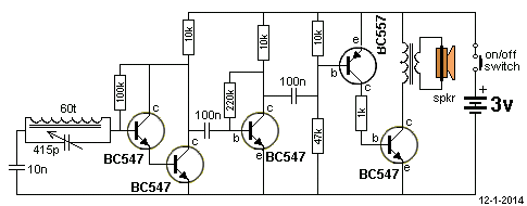
Here is a circuit that may look complex, but it shows
exactly what we are talking about.
It is an AM radio of 1980.
The signal from the tuned circuit may be 10uV and 1uA and the first
transistor of the Darlington Pair improves this by a factor of about 100.
The Darlington configuration turns two transistors
into a single transistor with enormous gain.
It puts very little load on the tuned circuit and does not affect its
ability to tune distant stations. This stage is connected to
the next stage with 100n capacitor and the output of the second stage is
connected to a driver/output that has a low input impedance. The main
purpose of the final section (consisting of two transistors) is to amplify
the current to drive the speaker transformer.
These are all the things we are discussing and the circuit is/was a
practical example of an AM radio, in the days when AM sold millions of
"Pocket Radios."
Normally, one stage is connected to next with a capacitor and most of the calculations are
done by determining the resistance (capacitive resistance - called
capacitive reactance) of the capacitor at a specified frequency.
But no-one has explained what is actually going on with this connection
and why this interfacing is very inefficient. The only reason why most
circuits work is due to the high gain of the transistors and even though
the biasing and coupling of stages removes a large amount of energy, the
final result of two stages is quite impressive.
The first thing you have to understand is this: The transistor in the
first stage does not "push" or "drive" energy to the next stage.
When the transistor turns OFF, the voltage on the collector LOAD rises
and this rise, associated with the current that can be supplied by the
load resistor is passed to the next stage.
For instance, when a 10k resistor has 5v across it, the current
capability of the resistor will be 0.5mA. But if the stage
is sitting at mid rail, this current is 0.25mA.
As the collector voltage rises, the voltage across the load resistor
reduces to say 1v, and the current capability reduces to 0.1mA
You can see the real current from the stage is a lot less than expected.
What we are talking about is a package of energy from one stage to the
next. This has never been discussed before and that's why no-one
understands how "combining stages" works.
Of course it is much better to DIRECTLY COMBINE STAGES, but this is
sometimes not possible and other times it requires a lot of circuit
design.
This packet of energy is transferred to the next stage via a capacitor
and the capacitor will always have a voltage across it as one stage is
at mid-voltage and the other will have a low voltage on the base.
As the voltage on the load resistor decreases, less and less current is
available from the load resistor and this means the capacitor gets
charged slower and slower.
But at the same time it gets charged and so the rise on the top plate of
the capacitor does not pull the bottom plate as high. So a lot of the
energy goes into charging the capacitor and the following stage does not
see much of the energy.
When the transistor in the stage we are studying is turned ON, the
voltage on the load resistor increases and the voltage across the
coupling capacitor reduces and the capacitor is put into a
"discharging condition." If you slowly reduce the voltage on the top of the
capacitor, it will discharge by delivering its energy into the base of
the transistor. But as soon as the voltage on the lower plate of the capacitor reaches
0.55v, the current into the base ceases as the base does not accept any
current when the base falls below 0.55v.
This means you might still have voltage (and energy) across the
capacitor that has not been removed and when the next cycle takes place,
the capacitor is already partially charged.
This means the capacitor will not be able to transfer the same amount of
energy as in the first cycle and that's why the capacitor becomes such a
poor transfer component. A resistor between base and zero volt rail will
improve this is the answer to why they have been included.
And that's why you will find some of your circuits DON'T WORK AT ALL.
The only reason why the circuits work AT ALL is due to the high gain of
the transistor and all these losses bring the final gain of many stages
to about 70.
You have to be able to visualise this action to see why your circuit is
not performing as well as expected. Especially when high currents are
involved.
Most data sheets show transistor gain at 1mA or 10mA. When you
increase this to 100mA, the gain drops considerably. That's why NOTHING
can be calculated.
It is pointless doing any calculations as you have no idea of the gain
you will get from each transistor or the value of the current-capability of the
input signal or the impedance of the stage that
follows.
If I could design a circuit with pen and paper, I would be a
multimillionaire.
Things can work out much better than expected or not work at all. And
it's when they don't work, that skill comes in - something that no
University course has ever touched-on, because they have never had to
design ANYTHING.
There is no skill in designing a circuit. The skill is getting it to
WORK.
MORE ON THE H-BRIDGE
I did not want to go further into discussing the H-Bridge but the instructors on YouTube are so incompetent at designing this stage that I want to cover the steps you need to follow so you see how inept the instructors are.
You cannot design a stage UNTIL you get some external values. They have NEVER designed a circuit in their life and their approach is completely impractical and shows no understanding.
The first thing you need to find out is the impedance of the stage you are driving as it will affect all the values of the H-Bridge stage.
This is also called the input impedance and/or the base-emitter impedance or some value in the range of 500 ohms to 5,000 ohms.
The self-bias stage we are designing is called a small-signal stage but what this really means it is a low current stage.
It can be from 0.1mA to 5mA.
You cannot design the stage and then connect it to a following stage as the output of the self-biased common emitter stage will be reduced and you will be very disappointed.
The collector LOAD resistor has to be equal or less than the impedance (resistance) of the following stage.
That's because the load resistor delivers the amplitude and if it has the same resistance, only about 50% of amplitude will be delivered. This is because the collector resistor and the coupling capacitor and the input impedance of the following stage forms a voltage divider.
But we cannot make any predictions because the real way to look at the transfer from one stage to the other is via ENERGY TRANSFER. And this involves analysing the circuit.
Next you need to work out the value of the emitter resistor and base-bias resistors to get the transistor to sit with the collector at mid-rail.
The bleed-current through the base resistors can ne 1/100th the collector current.
Next you need to work out the value of the emitter-bypass capacitor (electrolytic) to give a gain of 50 to 70 for the stage (to make it worthwhile). To do this you need to know the frequency you will be amplifying.
Normally it is at least 1/10th the resistance of the emitter resistor. If the emitter resistor is 1k, the capacitive reactance of the by-pass electrolytic should be 100 ohm at the desired frequency.
Next you need to know the current-capability of the input signal and it has to be at least 1/50th the collector current of the stage we are designing..
This is just the beginning of the parameters you need to start designing.
If you think the values are acceptable, I would not even waste my time doing any calculations.
Time is far too valuable.
Build the circuit and adjust the values to get the required results.
You can try working out the values mathematically and when you build the circuit you will see how incorrect your values were.
Here is a typical problem.
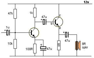
We have two stages. Each
stage has been correctly designed with the first stage allowing the
collector voltage to rise to 12v and fall to almost zero when the stage
is not connected to the emitter-follower stage.
In other words we have full rail voltage amplitude and we know the
emitter-follower stage has a high impedance.
But the term "high impedance is relative. It has 100 times higher
impedance than the 8R load.
This might not be a high impedance as far as the first stage is
concerned.
We have already mentioned the first stage does not "push" energy to the
second stage. The transistor turns OFF and the 1k load resistor
passes energy to the emitter-follower.
When the transistor turns OFF, a voltage-divider is formed with the 1k,
the 47u electrolytic and the input impedance of the emitter follower.
The 47u is about 2 ohms and the input of the emitter-follower is 800
ohms.
Let's say it is 1k and 1k. This means half rail voltage will appear on
the base and thus the emitter follower will only rise to 6v. We know the
speaker will receive up to twice this swing but if you are expecting
something like 24v, you will be mistaken.
The two stages have not been correctly matched and even though the first
stage is taking more than 10mA, it is not only the current-flow that has
to be correct, but the value of the collector LOAD.
Matching these two stages involves a PNP stage:
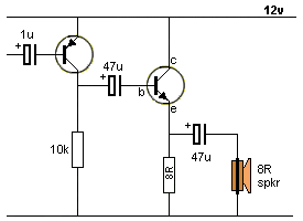
The first stage uses a PNP
transistor and it can raise the voltage to 12v and when it is turned
OFF, the voltage will fall to 0v. The next thing you have to work on is
discharging the 47u on the collector of the PNP transistor.
That's a topic for another discussion.
If you want to see the solution . . . click
HERE
All circuits work on the principle of
VOLTAGE DIVISION. Components are "dividing up" the available voltage and
that is how and why I can "see" a circuit working. The real way to lean
and understand "circuit design" is completely different from any
lecture, text book or discussion.
You have to be "guided" into seeing a circuit working and see that a
particular circuit WILL NOT WORK. This does not involve mathematics. It
does not involve calculations, other than a simple understanding.
Here's what you need to remember:
1mA flowing through a 1k resistor will produce a voltage drop of 1 volt.
From there, you just multiply and divide:
10mA will produce a voltage drop of 10 volt.
1mA through 10k will produce a voltage drop of 10v.
Similarly: A 1k resistor on a 10v supply will pass 10mA.
10k on 10v will pass 1mA
And once you remember the above, you continue with voltage division.
A 10k and 10k in series on 10v will produce 5v at the join.
1k and 1k on 10v will produce 5v at the join.
3k3 and 3k3 and 3k3 in series on 10v will produce 3v3 and 6v6 at the
joins.
And there is another area of electronics that Universities do not cover.
It's how to fix things.
All my projects include a section: IF IT DOES NOT WORK. I
teach how to fix a project.
Universities don't cover this topic because they have absolutely no idea
how to fix anything. That's why the piece of paper they hand you at the
end of 4 years is ABSOLUTELY WORTHLESS. One University graduate
came for a job application and said: Oh, I don't do soldering !!!
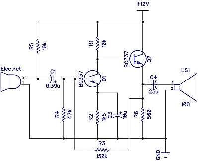
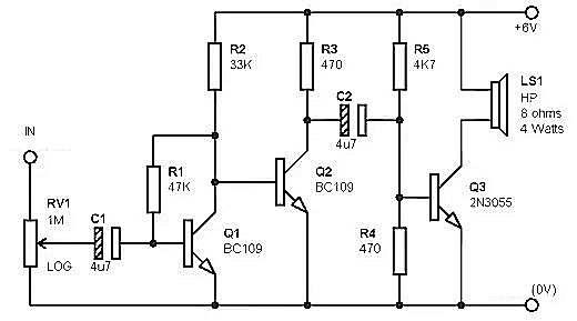
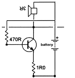
The circuit above is a 3-transistor
amplifier and the first thing you will want to know is the output
wattage.
You can see this amplifier will have NO output AT ALL. The BC337 is
being pulled up by a 4k7 and this will be converted to 470R or maybe
200R via the gain of the transistor and this value will be part of the
voltage divider network with the 8R speaker.
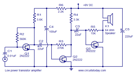
Here is a circuit that the designer thought would give a good output.
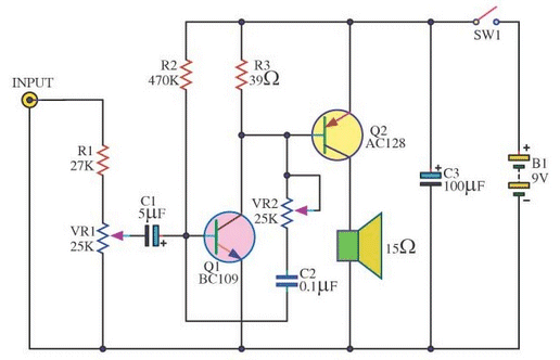
Here's a 3-Transistor amplifier and the first thing you ask:
"Where is the fault?"
Another faulty circuit.
To make it easy
we have removed all the components that are effectively "out of circuit"
as the top transistor is not turned ON.
But the 100u electrolytic is charged to about 6v, and it effectively
becomes a battery, so we have changed it to a battery:
Now you can see the base and emitter are both connected to the same
voltage and nothing is turning ON the transistor!!
You can now see the fault in this design. The 25u is going to take a
long time to discharge through 660 ohms of resistance.
Don't worry about the old-type of transistors.
It does not matter if you use a power transistor, the output of a
circuit will be controlled by the surrounding components.
And now we have a circuit that has a different fault.
This circuit has a surprising feature. The base of the upper transistor
is connected to the output of the circuit and when the bottom transistor
turns ON, the 470u electro will charge and this charging current will
flow through the speaker, The top transistor is turned off during
this time by the action of the two diodes. The 470u is now fully charged
and the current through the speaker is zero.
PUSH PULL AMPLIFIER
Here's an amplifier with an unexpected feature. It is the connection of the
base resistor to Q2. Instead of it being connected to the positive rail,
it is connected to the speaker.
The electrolytic can be thought-of as a battery to make the circuit easier to
understand.
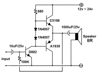
THE BLOCKING OSCILLATOR
The limiting factor of the amplifier is the 680R resistor. The PNP
transistor will be pulled down to the negative rail as hard as possible
via the driver transistor, so this part of the cycle will work. It will
be like pulling down with a 10R resistor. But the NPN transistor will be
pulled high via the 680R and this effect will be a lot weaker than the
other section.
We have explained that a transistor effectively converts the base
resistor to a smaller resistance by a factor equal to the gain of the
transistor. The gain in this circuit will be about 50, for the power
transistor, and the 680R will be converted to 13 ohms.
We will assume the 1,000u has an impedance of one ohm.
The circuit now become a voltage divider of 14:8 so that the
speaker gets 36% of the supply voltage. The way to find this
percentage is to add the total resistance in the circuit (14 + 8 = 22)
and the speaker will get 8 parts of this total. The equation is:
8/22 = 36%
You can see the speaker gets nothing like 100% of the energy of the
amplifier and although the output will be quite loud, the amplifier is a
very inefficient design.
This is how you look at a circuit and instantly work out its
performance. A simple voltage-divider equation will get a very accurate
value. 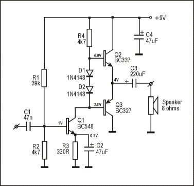
Even if the BC338 acts like an 8 ohm resistor, the speaker will get only
50% of rail voltage and so both parts of the push-pull arrangement have
to be very low impedance to get the full energy from the circuit.
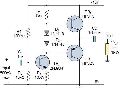
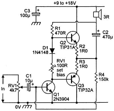
Look at the data sheet and you will find the transistor are RUBBISH.
The collector-emitter voltage is 4v and the gain is less than 50.
The TIP31A is going to be effectively 1,000/50 = 20 ohms and you are
going to lose 4v. So you have 8v divided between a voltage-divider of
20:16 and you might get 4v across the speaker.
That's why power amps start with a high voltage - to get the
output wattage.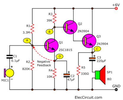
The fault lies in the 330R across the 220u electrolytic.
The transistor can charge the 220u and drive the speaker, but when the
transistor turns OFF, the speaker, 220u and 330R are in a "loop" and the
330R is going to take a very long time to discharge the 220u.
This means the transistor will turn ON in the next cycle and the 220u
will already be 90% charged from the previous cycle and the transistor
will only be able to deliver 10% or less of its energy.
Without doing any complex maths, the capacitor will take 8 milliseconds
to discharge to half voltage and if the frequency of the amplifier is
1kHz, the cycle-time will be 1 millisecond. You can see the
capacitor will discharge only a very small amount in this time.
You can see Q3 is being pulled HIGH by Q2. But what is pulling Q4
LOW??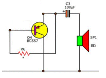
The fault lies in the direct-connection of the two transistors across
the supply. When the first transistor turns ON, the current through it
will be very high and this current will flow through the emitter-base
junction of Q2 and will be much higher than the transistor wants or
requires. The transistor may be damaged.
You must always put a current-limiting resistor in any path with these
features. A 1k resistor will limit the current and not
affect the operation of the circuit.
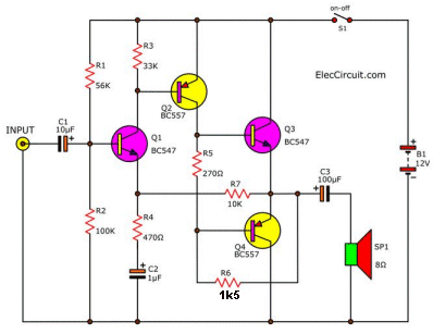
The 4k7 is going to be converted to a 50 ohm resistor by the gain of the
2N3055 (or even a higher value). This mean the speaker will see less
than 1v across it when in the idle state. The rest of the circuit can
only have a very small effect on turning ON the transistor via the two
470R resistors. The base is at the join of these resistors so the effect
will be very small. You would see less than 2v swing on the output. The
circuit is so inefficient that it is not worth working out any actual
values.
The 22u capacitor connected to the base of the driver transistor will
turn the transistor ON when it gets charged by the 3k3, but when Q2
turns ON, the whole 22u will drop a small amount and when it drops by
0.7v, the voltage on the base of the output transistor becomes zero and
the transistor is turned OFF. The 22u can drop further and further but
the output transistor is already turned OFF and this will have no effect
on the circuit.
As it drops further and further, it will be discharged a very small
amount by the 15k base resistor but this will leave it partly charged
and the following cycle will have very little capability to charge it.
This means the electrolytic will pass very little energy to the output
stage and the circuit will be almost worthless.
![]()
3-TRANSISTOR AUDIO AMPLIFIER
The driver transistor now turns OFF and releases its grip on the whole
of the output and the bottom output transistor is allowed to rise. The
"pulling-down" effect of the two diodes disappears and we just have the
top output transistor, the fully charged 470u and the 1k base resistor.
The 470u is like a 9v battery
This produces a surprising effect.
We start with Q3 turned ON via Q1 and the speaker receives current as the 470u
electrolytic is charging. Eventually it will have a voltage almost equal to rail
voltage across it. During this time, Q2 will not be turned ON because the D1 is
keeping the base LOW.
Q1 starts to turn OFF and this puts less "pulling effect on the base of Q3 and
the transistor starts to turn off because basically the emitter lead will not
rise because the 470u is changed.
However the base of Q3 can rise and D1 allows the base of Q2 to rise via the
470R resistor. This turns ON Q2 and the emitter follows the base and pushes the
470u higher. This keeps occurring and the speaker "flips over" and now
the current flows in the other direction and this pushes the cone in the
opposite direction.
Normally, when the transistor modes to wards the supply rail, the voltage across
the base resistor reduces and the transistor has less effect. But by
connecting the resistor to the speaker, it still keeps the transistor turned on
until the electrolytic is discharged. This produces slightly better performance
than if the base resistor is connected to the supply rail. 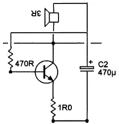
This circuit uses a capacitor that is not connected to either rail and
continues our discussion.
The circuit is called a BLOCKING OSCILLATOR to give it a name
everyone can remember.
ooooo00000ooooo
These circuit faults give you some idea of what to avoid when designing
an amplifier. You must build the circuit and test it before putting in
on the web for everyone else to criticise.
Page-1 Common-Emitter stage Go to
Talking Electronics
website
19/4/2024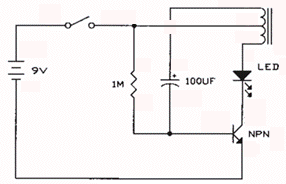
BLOCKING OSCILLATOR
It is really a FEEDBACK OSCILLATOR as the winding from the transformer
provides POSITIVE FEEDBACK that turns the transistor ON fully - actually
more than fully - and it becomes SATURATED and even SUPERSATURATED.
This is all part of the first half of the cycle and now the important
thing to understand is this:
How does the cycle produce the second half of the cycle?
It is the 100u electrolytic.
But first we have to understand how the transformer works,
The transformer has two windings and we say the winding connected to the
LED and collector is the primary and the winding connected to the
capacitor is the secondary. It does not matter how many turns on
either winding as long as the transformer works in the circuit.
Here is the point to understand:
When the transistor turns ON, the centre tap will see 9v and the winding
connected to the LED will have a lower voltage. It does not matter
how much lower but you can see the voltage decreases as you move down
the turns on the diagram.
This means the voltage on the secondary winding will have a higher
voltage as you move up the diagram.
When the switch is closed, the 100u will be uncharged and the positive
lead of the electro will see 9v. This will pull the negative lead of the
electro UP and because the base cannot rise higher than 0.7v, the
positive lead will not rise higher than slightly more than 0.7v. This
means the secondary winding will not be higher than 0.7v but it will
deliver a current to the electro that will charge it.
This charging current will pass through the transistor to turn it ON and
illuminate the LED. This current will be very high and as there is no
current limiting resistor in the circuit, the LED will be damaged.
That's why this circuit is so disastrous. However let's continue.
The electro will keep charging and as it charges, the current into the
base of the transistor reduces.
A point is reached where the current is not able to keep the transistor
fully turned ON and it turns OFF a small amount.
Now, here's the point to understand.
The magnetic flux in the core of the transformer is a maximum and now
the current is reducing. When the current reduces, the magnetic flux
starts to collapse and this produces a voltage in the secondary winding
that is of opposite polarity. This means the positive lead of the 100u
sees a slightly lower voltage and since the electro is charged, the
negative lead falls by the same amount.
This puts a lower voltage on the base and it only has to drop by 0.15v
and the transistor is fully turned OFF.
That's what happens. The transistor turns OFF. The transistor
disappears from the circuit and there is nothing to discharge the 100u.
That's where the 1M resistor come in. It discharges the electro very
slightly so that the negative lead has 0.7v on it and this turns the
transistor ON again.
This puts a high voltage spike on the positive lead that makes the
electro charge and this turns the transistor ON more to create the next
cycle.
Page1A. more on the stages
Page-2 emitter-follower - common collector stage
Page-2A common base stage
Page 4 More on Coupling Stages
Page-5 The FLIP FLOP
Page-6 All the "YouTube" mistakes
The
REAL
Transistor Amplifier