Try this test and see if you get 100%.
We are using a simple NPN or PNP transistor such as BC547, BC557 or BC338.
Not all the answers have been covered in the lecture-notes.
The Test is to see how much you know.
After completing the test you can find some of the lecture-notes here:
Link 1
Link 2
Link 3
1. Transistors are separated into two types. Name them.
Positive and Negative
P and N
PNP and NPN
PNN and NNP
2. Name the three leads of a common transistor:
Collector Bias Omitter
Base Collector Case
Emitter Collector Bias
Collector Base Emitter
3. Which way do you normally draw an NPN transistor in a circuit:
a
b
c
d
4. When testing a transistor with a multimeter, it is set to:
Volts
Low Ohms
High Ohms
High Volts
5. Name the leads of a transistor:
a
b
c
d
6. The easiest transistor to test is:
PNP
NPN
Both equal
7. The lead marked with the arrow is:
The Collector
The Base
The Emitter
The case
8. If the voltage on the base of a transistor increases, does it:
Turn on
Turn off
Not enough information
Remain the same
9. Which diagram is correctly identified:
a
b
c
10. Which circuit is called a self-biased stage:
a
b
c
d
11. Which transistor is being turned ON in an amplifying stage:
a
b
c
12. In the diagram below, what will happen to the pointer when a finger is
applied to the leads:
The pointer will move across the scale
The pointer does not move
13. In the diagram below, name the fault with the transistor:
The transistor has shorted between base
and both other leads
The transistor has shorted between collector and emitter
The transistor is not faulty
14. Which circuit is correctly biased:
a
b
c
15. Which circuit contains an input capacitor:
a
b
c
d
16. When a transistor is turned ON, it is like:
a
b
c
17. The 1k resistor is changed to 2M2, the collector voltage will:
rise
fall
remain the same
18. Transistor stage B is called:
H-Bridge
self biased
resistor bridge
19. The stage is called:
DC coupled
AC coupled
Direct Coupled
20. When the input signal is rising, the output is:
falling
rising
unknown
21. The input capacitor is 100n, you would design the output capacitor to be:
1n
10n
100n
1u
22. Putting another 2M2 across the base-bias resistor will:
increase the collector voltage
decrease the collector voltage
collector voltage will remain the same
23. A transistor has a gain of 350 in the circuit above. Replacing it with a
transistor having a gain of 150 will:
increase the collector voltage
decrease the collector voltage
collector voltage will remain the same
24. The base-bias resistor falls off a module. The collector voltage of the
transistor in the circuit above will:
increase
decrease
remain the same
25. The collector resistor falls off a module. The collector voltage of the
transistor in the circuit above will:
increase
decrease
remain the same
26. The gain of the transistor is 250. What is the gain of this self-biased
stage:
250
70
22
Note: The gain of a self-biased stage is about 70 for all types of transistors as
the 2M2 reduces the gain.
If you want to reduce the gain, you can add a resistor to the input or decrease
the input capacitance:
Changing the input components will reduce the input signal and thus reduce the
gain of the stage.
27. Which stage will produce the highest gain:
A
B
both the same
Note: The base-bias resistors for circuit 27B reduces the input signal
considerably and that's why the output will be less than 27A.
28. What is the gain of this H-bridge stage:
10k
Depends
on the gain of the transistor
1,000
1
Without the electrolytic, the gain is 10. With the electro the gain is whatever
the transistor can achieve.
29. Which stage has the highest input impedance (resistance):
H-bridge
self-biased
both the same
30. The transistor is equal to a resistor of:
1k
10k
6k
31. The voltage on the collector is 1v. To increase the voltage, the 1M is:
increased in resistance
decreased in resistance
the collector voltage cannot be changed
32. The output capacitor should be about 10 times larger than the input
capacitor. The reason:
the output will have a higher current
the output will have a higher voltage
no technical reason
Note: A higher current will allow a capacitor to charge faster. We do not want a
coupling capacitor to charge as this will reduce the amplitude of the signal.
The output will have at least 10 times more current and so a larger capacitor
will take longer to charge.
33. Can you design a self-biased stage without knowing the characteristics of
the input and output LOAD:
yes
no
not relevant
Note: You MUST know the characteristics of the input device and output LOAD as
these will control the amplitude of the signal produced by the stage.
34. The signal on the collector of a self-biased stage is 1,200mV. When a LOAD
is connected to the output, the amplitude of the signal will:
decrease
increase
stay the same
Note: A waveform (amplitude) produced by a stage will ALWAYS decrease when the
output is connected to a LOAD.
35. The input capacitor is reduced to 10n. The signal on the collector will:
decrease
increase
stay the same
Note: The signal on the collector may stay the same but theory says it will
decrease. That's why coupling capacitors are as large as possible.
36. Using our theory with decoupling capacitors, what size capacitor will be
used for C3:
100n
1u
10u
Note: Increasing the value is good design and shows good circuit knowledge.
Maybe 10u is too high.
37. Using our theory on stage amplifying, for each stage, what do you think
will be the gain of the circuit in Q36:
4,900
70
200
Note: The gain can be as high as 70 for each stage. But when the amplitude
reaches full rail voltage the signal will not increase.
38. Can this circuit amplify a signal as small as one micro-volt:
yes
no
Note: The circuit will detect a signal as small as one micro volt because it is
already "turned ON" and will detect "hum" in leads and all noise on the input.
39. Is it important to have the collector voltage equal to mid-rail voltage:
yes
no
Note: When the collector voltage is mid-rail, the stage can produce the maximum
output without "clipping" or "bottoming" or distorting a signal.
40. In an audio amplifier, does it matter if the signal emerges INVERTED:
yes
no
Note: Your ear cannot detect an inverted signal.
41. What is the input impedance of a self-biased common emitter stage:
5,000 ohms
1,000 ohms
cannot be determined
Note: All the answers above are correct. The input impedance (resistance)
changes enormously, according to the value of the base-bias resistor.
As the base gets turned ON harder with a low value base resistor, the input
resistance decreases enormously.
Here is how to consider the value.
In the circuit above, the base has a 2M2 resistor and 3v supply. This means less
than 1 microamp is entering the base and thus another microamp (or less) will be
detected by the stage.
This is all you have to know.
42. What happens to a 1v input signal because we know the base will not rise
above 0.7v:
The signal gets converted to current
The
signal gets converted to voltage
cannot be determined
Note: As the input signal increases in amplitude, it will deliver a higher
current and this is what the transistor will detect as the voltage on the base
will rise very very little. So it does not detect the voltage, ONLY the current.
43. How does the signal from the electret microphone enter the base of the
transistor:
The signal gets converted to current
The
signal gets converted to voltage
The
signal enters as voltage
Note: The electret microphone detects a whistle and produces a wave very similar
to a sinewave. When the FET transistor inside the microphone turns OFF, the
voltage on the left lead of the 100n coupling capacitor rises. This voltage
passes through the capacitor and adds a little more current into the base.
This because the voltage is higher than the 0.65v on the base.
The transistor reacts to this extra current and allows 200 times more current to
flow in the collector-emitter leads. This reduces the voltage on the collector.
Connected to the collector is a 2M2 resistor and now a slightly smaller voltage
will appear across the 2M2 and thus it will deliver slightly less current into
the base.
This means the base will see slightly less current and so the transistor will
not perform to the full extent of 200 times amplification. Normally we allow the
gain to be 70.
This means the output waveform will be 70 times larger than the input waveform
and will be inverted.
You cannot perform any mathematical calculations because you don't know how much
"degenerating effect" the 2M2 will have on the signal.
Degeneration is the name we give to an effect that improves stability. It can
also be called NEGATIVE FEEDBACK.
44. Does the first transistor pass energy to the second stage:
yes
no
unknown
Note: NO. When the first transistor turns OFF, the 22k pulls the 100n high
and delivers energy to the second stage.
When the first transistor turns ON, it pulls the 100n low and turns OFF the
second stage. It is the 22k resistor that does all the "passing."
45. What effect does a coupling capacitor have on the transfer of energy:
none
a lot
unknown
Note: The effect is unknown. Passing energy into the base of a transistor
is not a linear transfer. As the transistor becomes more saturated, the gain of
the transistor reduces.
It is amazing that we can get a reasonable linear and undistorted outcome from
so many non-linear features.
However a capacitor does not transfer 100%. There are a lot of losses and the
high-gain of each transistor overcomes these losses.
But it can transfer "a lot."
46. Why does a coupling capacitor have losses:
because
it charges
because
it discharges
unknown
Note: When a signal passes through a coupling capacitor, it charges.
This means the voltage across the capacitor reduces the amplitude of the signal.
When the amplitude reduces, the current provided by the signal reduces and since
the transistor operates on CURRENT, the transistor sees the capacitor as
producing losses.
47. Can you determine coupling capacitor losses:
yes
no
Note: The answer is Yes and NO. You can try to work out the losses but
they increase and decrease according to the frequency.
The losses are due to the capacitor charging during each cycle and the more it
charges, the higher the losses.
You cannot choose a single capacitor value for the range 20Hz to 20,000Hz and so
you have to compromise.
You need a high-value capacitor when high currents are involved and if a high
voltage is involved, this adds to the size of the capacitor.
And if a high current is flowing in and out of the capacitor, it must have a
high ripple capability so it does not get hot.
48. How much current is going to turn the stage ON fully and turn it OFF
fully:
2uA
and about 1.5uA
2mA
and about 1.5mA
unknown
Note: We cannot work out the values accurately because the operation of the
stage is not linear, but the base current is about one microamp flowing through
the 2M2 resistor and if the transistor has a gain of 200, the collector current
will be 200uA. This current will produce a voltage of 0.0002 x 20,000 = 4v = the
theoretical voltage across the 22k resistor. This means the 22k will have to be
reduced to 10k for the collector to sit at mid rail. Or the transistor has to
have a gain of 100.
An additional 1uA will turn the transistor ON fully and about 1uA will turn it
off. The values of "2mA and about 1.5mA " are far too high.
49. Why is the H-Bridge stage a bad choice for a pre-amplifier::
it has a low input impedance
it will have a small amplification-factor
it uses more components than the self-biased stage
Note: All answers are correct. The input impedance is controlled by the 47k resistor on the base for
rising input signals and this reduces the input impedance by an unknown amount -
it could be as high as 50%. The rest of the circuit will have the same gain as
the self-biased arrangement.
Both circuits have a degeneration factor to keep the collector at about mid-rail
voltage if the supply rises or falls by a small amount.
In the H-bridge arrangement the degeneration is the created by the emitter
resistor.
50. If the rail voltage is changed from 3v to 5v, will mid-rail voltage on the
collector be maintained:
yes
no
unknown
Note: Mid-rail voltage will be maintained reasonably successfully by the action
of the "feedback" 2M2 resistor on the base.
If we replace the transistor with a variable resistor we see the resistor must
be 22k in both circuits for the voltage on the collector to be mid-rail. This is
a simple voltage-divider analysis.
This is how it is maintained:
When the rail voltage increases by 2v, we will take things very slowly. We will
assume the collector voltage rises 2v. This will put an additional 2v across the
2M2 and cause a higher current to flow through this resistor. This extra current
will flow into the base of the transistor and make the transistor turn ON more
and reduce the collector voltage.
This is all the transistor can do and the voltage on the collector will reduce a
small amount, but not necessarily exactly 2v. That's the best the
transistor can do.
It cannot come down the full 2v because the transistor has to be turned ON more
to allow extra current to flow in the collector-emitter circuit due to the
higher rail voltage. And this extra voltage has to appear across the 2M2.
51. How do you design a self-biased stage. What is the collector current:
1mA
0.1mA
10mA
Note: The collector current should be as small as possible because higher
currents produce "transistor noise."
52. How do you select the collector load resistor
choose any value
22k
2k2
Note: For a self-biased pre-amplifier stage, select 0.1mA for collector current.
This is the current flowing through the collector LOAD resistor.
The voltage across the resistor will be half-rail voltage.
For each one volt across 1k resistor, 1mA will flow.
This means 0.1mA will flow in 10k resistor and 1mA through 22k for 2.5v
53. How do you select the base-bias resistor:
choose any value
220k
2M2
Note: Build the circuit and fit 220k. The collector voltage will be too
low. Increase the base-bias resistor until the collector voltage is mid-rail. It
will be about 2M2 to 3M3. No mathematics required. You cannot work it out
mathematically as you
don't know the gain of the transistor.
I have never mentioned the 0.7v base-emitter voltage because it is not
important.
It is a feature of a transistor that is turned on and conducting. But it is so
small that you can neglect it in every decision.
54. What amplitude waveform will the self-biased pre-amplifier stage amplify:
any amplitude
1mV to 1v
0.1mv to 3v
Note: The circuit will definitely amplify a signal with an amplitude as small as
0.1mV and as a pre-amplifier, the signals are generally about 10mV, 100mV and up
to 3v.
The stage will have a gain of more than 100, but when it is connected to another
stage, this gain will reduce and we generally allow a value of 70.
55. What will happen when a 100 ohm magnetic sensor is connected directly to
the base of a self-bias stage:
the circuit will not amplify the signal
the circuit will amplify the signal
the output will be 700mV
Note: The circuit will not amplify the signal because the voltage across the 100
ohm coil will be very small - much small than 650mV needed to turn the
transistor ON.
The 2M2 normally allows the transistor to produce this voltage, but that is
because nothing is connected to the base.
A capacitor connected to the base will get charged by the 2M2 and the transistor
will see 650mV.
But 100R in series with 2M2 and a supply of 2.5v, will produce only a few
millivolts across the 100R.
The magnetic sensor must be connected to the base via a capacitor as per the
following circuit:
Fig 55a
56. What will be the output from fig 55a:
the circuit will not amplify the signal
unknown
the output will be 700mV
Note: The capacitor will allow 650mV to be developed on the base and the
transistor will amplify the 10mV signal about 70 times to produce 700mV output.
As soon as the base has about 650mV developed on it, the transistor will amplify
all signals from 1uV to 3v or higher.
57. What happens if the input signal is higher than 5v:
only about 0v to about 50mV of the signal will be processed
the stage will process the signal
only 0v to 5v of the signal will be processed
Note: This is a very complex question because this amplifier is designed for
very small amplitude signals. However it will process all amplitudes and
as soon as the amplitude delivers more than 2uA, the transistor will then be
saturated and it will be turned ON fully. If the input signal continues to rise,
the output signal will not change. This means only a very small part of the
signal will conform to the input, however the distance between each peak and
each minimum will be seen on the output and this will provide the frequency of the signal.
The signal will be distorted as shown in the following graphs:
Since there is very little difference (to the ear) between a sinewave and a
square wave, the signal will be considered to be processed.
The 100n coupling capacitor will absorb the signal and charge to 6.3v
That's because the base can never rise above 700mV and the rest of the amplitude
has to charge the capacitor.
58. The electret microphone is connected to a separate 3v power supply and is
connected to the self-biased pre-amplifier via two 100n capacitors. Will it
work::
yes
no
only if the microphone has a 5v supply
Note: The left side of each 100n can be any voltage. Only the change (amplitude)
of the signal is detected by the base of the transistor. And the capacitor
connected to the 0v rail is connecting the two circuits together. The amplitude
of the signal will be less due to the 0v rail capacitor but the amplifier will
produce and accurate amplification.
59. Can a piezo diaphragm be connected directly base of a self-biased
amplifier:
yes
no
a 100n coupling capacitor is needed
Note: No coupling capacitor is needed as the piezo diaphragm is really a 22n
capacitor and the transistor gets its 700mV base voltage from the 2M2 resistor
and it will amplify the waveform from the piezo when it is tapped. A 100n
coupling capacitor is only needed to make sure the transistor gets its 700mV
"turn ON" voltage.
60. Can a piezo and magnetic sensor be connect to the input at the same time:
yes
no
Note: The two transducers (detectors) can be paced on the input and the circuit
will work with slightly less sensitivity as the signal will be sent to the other
detector and some of the energy will be lost.
60A. When we talk about the "gain" of a transistor, is this
the voltage gain
the current gain
60B. Is the "gain" of a transistor constant
yes
no
Note: The gain of a transistor reduces when a higher current flows
60C. Can the "gain" of a transistor reduce to 1 (having no gain)
yes
no
Note: The gain of a transistor reduces to 1 when it is oscillating at its
maximum frequency or when the current is higher than the transistor can handle.
REVISION
When comparing the H-Bridge amplifier with the self-biased stage, the
self-biased stage is simpler to design, has the higher gain, uses less
components, consumes less current, has a higher input impedance and is less
susceptible to noise from the supply because it has a higher-value load resistor
and a feedback resistor.
Both designs have an ability to keep the collector at mid-voltage when the
supply increases or decreases.
The self-biased stage is not covered in any University lectures or text books
because none of the instructors have ever built an amplifier circuit and have no
clue of the capability of any circuit other than a bridge amplifier. You need no
mathematical gobbledygook for this stage and a test question simply revolves
around building the circuit and fitting a base-bias resistor that suits the gain
of the transistor. You cannot work out anything before-hand. And a test question
is almost impossible to produce. So, you are missing out on the most important
amplifier in you career.
What is the order of design:
1. Select the supply voltage.
2. Select a transistor.
3. Decide on the collector current
The collector will see mid-rail voltage
The current through the load resistor should be 0.1mA to 3mA
for a pre-amplifier
For each volt across the load resistor and 0.1mA flowing, the resistance is 10k
For each volt across the load resistor and 1mA, the resistance is 1k
4. Select a base-bias resistor that produces mid-rail voltage on the collector.
5. Select 100n for input capacitor and 100n or greater for output capacitor.
6. The input device can have almost any resistance or impedance and any signal
from less than 1uV to 20mV.
In this range the output will not be distorted.
Here is the circuit:
Here is a totally impractical circuit from YouTube:
It might work but the voltage on the collector will depend on the gain of the
transistor (and the supply voltage) and if you use a different transistor with a
slightly different gain, the mid-rail voltage will change.
But the most important reason NOT to use this design is the noise it produces.
Any noise on the power rail will be amplified 200 times and passed to the LOAD
resistor. A small portion of this noise will be passed to the power rail where
it will be amplified another 200 times.
Our self-bias
arrangement has a feedback resistor that helps compensate for different
transistors and different voltages and acts against amplifying noise. Instead of
amplifying noise, the feedback resistor reduces it by about 10% to 30% and so it
is effectively removed. You will never see this design in any
practical application . . . because it so ineffective. So don't study it
or use it.
A question from a YouTube video:
How does a transistor amplify current?
A transistor is really a variable resistor and when it reduces resistance, (due
to more current being supplied to the base lead) a higher current will flow in
the LOAD resistor (or the device you have connected between the supply and
collector lead).
When we say the transistor reduces resistance, it actually allows more current
to flow in the collect-emitter circuit.
The transistor can also be placed in a configuration where it allows more
current to flow in the emitter-collector junction and through the device
connected to it. So you have to understand both concepts.
We have only covered the common-emitter stage . . . . only a fraction of the
total field.
There is an enormous amount of instruction and circuitry on
talkingelectronics.com website
with entirely new ways to see how circuits work so you can "see" them working in
your mind and be able to design and test them like an expert (like me).
Here is just a few links to start you in the right direction:
Link 1
Link 2
Link 3
THE TRANSISTOR AS A SWITCH
This another field of operation for a transistor.
It is still an amplifier but in a different mode called DIGITAL MODE.
This mode has two states. One state has the transistor fully turned OFF
and the other state has the transistor fully turned ON.
These two states have an amazing feature. In either state the transistor stays
the coolest or even coldest.
When a transistor is fully turned ON, the voltage across the collector-emitter
terminals is the lowest and the transistor dissipates the least heat.
Not only that, but each state is called a DEFINED STATE or an OBVIOUS STATE or a
dedicated state or a state that cannot be challenged or a state that is "known."
There are a number of names for these two modes (states).
ON and OFF
Digital Mode
CUT-OFF and BOTTOMING
"0" and "1"
HIGH and LOW
Conducting and Not-conducting
and the transistor stage can be called an
Inverter
It can also be called a SWITCH.
This stage or state is used to turn things ON and OFF. Not half-ON but
fully ON.
To put a transistor into this mode, you have to follow some rules.
The first rule is to allow 100 gain for LEDs and resistors as the LOAD.
For globes and motors the gain is 20. That's because a globe or motor
takes 5 times more current to get it to start to glow or start to turn.
You can now work out the base current, by dividing the collector current by 20
or 100.
You can deliver extra current but it will not
achieve anything and it will be wasted.
Q61. Will the globe illuminate:
yes
no
Note: Using the theory above, the 100mA globe requires about 500mA to make sure
it starts to glow.
The next factor to take into account is the gain of the transistor is only 50
when a high current flows.
This means the base current has to be 10mA. (10 x 50 = 500) With a control voltage of 5v, the resistor to the base has to be 5/0.01= 500
ohms. Select 470R resistor. The 1k in the circuit above should be 470R
Q62 Name the function of the following circuit:
amplifier
inverter
Note: In the context of this discussion, the circuit is an Inverter
Q63 In the circuit above, the current into the base will be about 5mA.
The transistor will have a gain of 100. What is the collector current:
500mA
12mA
Note: The collector current is limited by the value
of the LOAD resistor. Even though the transistor will pass up to 500mA, the 1k
resistor in the collector limits this to 12mA.
Q64 Will the circuit operate the motor:
yes
no
Note: The
motor will require 500mA to start revolving. The base will see 5/220 =
22mA. The transistor will amplify this to 22 x 50 = 1,100mA but the motor
only requires 500mA, so the circuit will work.
Q65 Will the circuit illuminate the two white LEDs:
yes
no
Q66 What is the collector current:
20mA
12mA
5mA
Note: LEDs have a characteristic voltage across them
when they are illuminated. This voltage depends on the colour and does not alter
for the brightness or size. For a white LED, the voltage is 3.2v
This means 6.4v is dropped "lost" across the LEDs and only 12 - 6.4 = 5.6v is
available as the supply voltage for working out the current through the circuit.
We now have 5.6v across a 1k resistor and this means 5.6mA will flow in the
collector circuit. The base will see 5/10,000 = 0.5mA and the collector
will deliver up to 100 x 0.5 = 50mA. This means the circuit will work.
The transistor can be used to control the flow of
signals and it can stop and start the flow. This is called GATING
and we have covered gating on talkingelectronics website:
In the first circuit, both inputs have to be LOW and if either input goes HIGH, the
gate changes from HIGH to LOW.
For the second circuit, both inputs must be LOW and both must go HIGH for the
output to change from HIGH to LOW.
The three 10k resistors have a purpose.
When the two inputs are LOW, the voltage on the voltage on the join of the first
and second 10k resistors will be 0.7v This would normally be high enough to
change the state of the gate. But the second and third 10k form a voltage
divider to produce mid-voltage of 0.35v and this is not enough to change the
gate.
This allows the input to rise to 1v and the gate will still not change.
The 0.3v allowance allows the inputs to be connected to the collector of a stage
and when the transistor in this stage is "turned ON" the collector-emitter
voltage will be 0.2v (we have a 0.3v allowance).
Q67 The motor requires 250mA to start and 50mA to run. Will this circuit
work:
yes
no
Note: No. The circuit will not work.
The BC547 transistor is only able to pass 100mA. The motor requires 250mA.
Secondly, the transistor will only have a gain of 50 when trying to pass a high
current and the circuit will only produce 0.5 x 50 = 25mA.
The circuit will not activate the motor, BUT . . . what will happen?
The transistor will pass about 50mA to 100mA and because the motor is not
rotating, it will not produce a back EMF and thus the stalled resistance of the
armature will pass the current. This means a very small voltage will appear
across the motor and thus more than 10v will appear across the transistor. When
you multiply the voltage and current you get nearly: 10x 0.1 = 1watt of heat
dissipation in the transistor and it will be destroyed.
Q68 The motor requires 250mA to start and 50mA to run. Will this circuit
work:
yes
no
Note: The circuit will work. The base current is 5mA and the BC338
will have a gain of 50, so it will deliver a maximum of 5 x 50 = 250mA.
You have to take the capability of the transistor into account when designing a
circuit.
When a transistor is fully turned ON, the voltage across it will be 0.3v to 0.5v
and this represent a wattage of about 25milliwatts.
If the motor is loaded and takes 150mA, the wattage will be 75milliwatts.
During "start-up" this loss will be much higher, but it is only for a very short
period of time.
Q69 If we increase the resistance of the LOAD resistor, will the
collector voltage:
rise
fall
remain the same
unknown
Note: The collector voltage will fall. This is the fact that we have
been covering in the above questions. When a motor is operating, its resistance
is effectively increased and the voltage across the transistor falls to the
lowest value. That's why the transistor remains cold.
Q70 Which stage do you think is the best design for a pre-amplifier:
H-Bridge
self-bias
You will be using the transistor very little as an amplifier in your electronics
designs and unless you can visualise it as a variable resistor, you will not be able
to do any real designing.
Universities, text books and YouTube videos have never gone further than the
common-emitter amplifier because they have not realised the variable resistor
concept and have never designed a circuit in their life. Go to
Link 3 for a discussion on the transistor as a variable resistor.
What is the "voltage gain" of a common-emitter stage?
Note: In 50 years of designing circuits, I have never been asked or needed
to know the voltage gain of a stage. A transistor works on amplifying CURRENT
and any voltage delivered to the base is converted to a current by the
transistor.
If you want to know how much current is required into the base of a transistor to
deliver 12v across the LOAD, a simple equation can be used.
Suppose the transistor has a gain of 100. For each 1mA into the base, the
collector will deliver 100mA. Each 100mA through the 100R LOAD will produce
[V=IR] 0.1 x 100R = 10v
So you need just over 1mA base current to produce almost rail voltage across the
LOAD.
Remember this: One amp flowing through one ohm produces one volt across
the resistor.
So, if you pass 100mA (that is one-tenth of an amp) across 10 ohms, the result
is one volt (you have divided one value by 10 and multiplied the other value by
10).
If you pass 100mA across 100 ohms, you produce 10 volts. No mathematics needed.
Just multiplication and division.
Q71 The supply voltage is gradually increased. At what voltage will the transistor turn-ON:
5v
21.8v
Note: Forget everything you have read about the input impedance of a transistor
being less than 10k. The input impedance is very high and it will detect current
as small as one microamp or less.
As the supply is increased, the small leakage current through the two zener
diodes will pass current to the base and as soon as 0.7v is developed across the
base-emitter junction, the transistor will start to turn ON. The supply can be
as low as a few volts and the zener voltages of 9v1 and 12v DO NOT have to be
developed across the zener diodes. This is called a ZENER LEAKAGE situation. As
the supply is increased, the leakage current will increase at a faster rate
because it is "diode leakage" but you can consider the two zeners as
high-resistance resistors.
Q72 A 680R resistor has been placed between base and 0v rail. The supply voltage is gradually increased. At what voltage will the transistor turn-ON:
5v
21.8v
Note: The 680R between base and 0v rail has changed the operation of the circuit
completely.
The 680R is a very low impedance compared to the input of the transistor and a
voltage will only develop across this resistor when a noticeable current is
flowing. When the supply reaches 9v1 + 12v = 21.1v the voltage across these two
zener will not be allowed to get any higher and so any increase in supply
voltage will be passed directly to the 680R and every 0.1v increase will appear
across this resistor. When the supply increases by about 0.6v or 0.65v or 0.7v,
this voltage will appear on the base of the transistor and turn it ON fully. It
must be noted that a further increase of 0.1v will blow up the transistor
because the supply voltage is being passed DIRECTLY to the base as the zener
diodes are RIGID ITEMS and do not allow a voltage higher than their marking to
appear across the leads.
The 680R has been added to make sure the circuit ONLY turns ON when the supply
reaches 21.8v
You can increase the 680R to 1k or 10k and the circuit will operate exactly the
same. That's because 10k is considerably smaller than the very high input
impedance of the transistor.
Almost no voltage will be developed across the 10k with "leakage current." It
takes "real current" to develop a recognised voltage.
And only "real current" starts to flow when 9v1 + 12v is developed across each
zener and they start to "break-down." In other words they become like a fully
extended shock absorber and any further extension will pull on the other end by
a direct amount as it is fully extended. That's the way the zener works.
As soon as it gets 9v1 across it, any increase will be passed directly to the
component below (that's not really correct as voltage develops across each zener
by about the same amount and when the total combined voltage is reached, the
next increase is directly passed to the component below)
This is a very good lesson on understanding "impedance." Impedance is used when
an actual resistance-value is not known and it changes when the current
increases. It's a value you cannot measure because test equipment will not
supply the exact same current (since resistance is determined with a
specified voltage and a certain current is flowing).
Q73 What is the function of this circuit:
amplifier
constant current
Note: The circuit delivers a constant current of 10mA to the LED when the supply
is between 5v and any other higher voltage.
The 10mA current is produced by the circuit by the 72R resistor and here's how
it works:
Place two ordinary diodes between the base and 0v rail. Use a "turn-ON" between
base and 5v rail. This can be any value from 1k to 10k or higher and only has to
pass one hundredth of 10mA.
Place any colour LED in the collector circuit and NO current-limiting resistor
is needed.
When
the circuit is turned ON, 0.7v will be developed across each diode.
The characteristic voltage across the base-emitter junction is 0.7v and this
cancels one of the diodes.
This means 0.7v remains for the emitter resistor.
If we want 10mA to flow through the LED, the same current must flow through the
emitter resistor.
From Ohm's Law: I=V/R
0.01 = 0.7/R
R = 0.7/0.01 = 70/1 = 70 use 72R resistor.
If you use 140R resistor the current will be 5mA
If you use 36R resistor the current will be 20mA
The circuit limits the current because the transistor is turned ON by the 4k7
and current flows through the 72R resistor and produces a voltage drop across
it. This voltage increases and increases until it reaches 0.7v.
The voltage on the base is 1.4v
The voltage across the resistor cannot increase to 0.8v because this will mean
there is only 0.6v available for the base-emitter junction and the transistor
will be "turned OFF."
So, only 10mA will flow as this will produce 0.7v across the 72R.
If the emitter resistor is removed, a very large, uncontrollable, current will
flow and the LED may be destroyed.
This is because the two diodes are equal to a 1.4v zener diode and when any
voltage below 1.4v is across it, the zener (the two diodes) do not
function and they are effectively OUT OF CIRCUIT.
This mean the 4k7 is connected to the base and the transistor will amplify the
base current 100 times and pass this current through the LED.
With no emitter resistor, the base will never rise above 0.7v and the two diodes
will have no effect.
You will notice all these calculations do not involve the supply voltage and it
can be almost any value as only a very small current is flowing.
Q74 What is the gain of this circuit:
100
1,000
10,000
Note: This circuit produces a very high gain and uses very few components. It is
difficult to get high gain with direct coupling and this circuit very reliable.
The only problem is the quiescent current is 5mA or 50mA, depending on the input
voltage.
The circuit is very difficult to test because the voltage on the collector of
the first transistor is either 0.3v or 0.7v and you will have to be able to
detect the difference.
Here's how to work out the gain.
The first transistor needs to be turned ON fully to bring the collector below
0.7v so the second transistor changes state.
This means the first transistor will pass 5mA through the 1k resistor.
The base will have to be supplied with 1/100th of 5mA.
To pass 5/100th mA through 100k, the input voltage must be: 1/00 x 100
x
5/100 x 1/1,000 x 100,000 =5v
If the gain of the first transistor is 200, the input voltage needs to be 2.5v
When the first transistor is OFF, the base of the 2nd transistor will have 1k.
This will allow 5mA into the base.
When the second transistor is turned ON, the current through the 100R will be:
5/100 = 5/100 x 1,000 mA = 50mA.
When 5mA flows into the base the transistor will be capable of multiplying this
current by 100 = 500mA.
But the load only accepts 50mA so the second stage has a gain of 10.
This means the overall gain of the circuit is 100 x 10 = 1,000
These are the sort of calculations you can carry-out in your head . . .
AND YOU NEED TO . . . .to be able to see if a circuit will function.
Normally this type of circuit uses high-value load resistors so the quiescent
current is very small.
Q75 When the collector voltage is too high, does the transistor:
break-down
zener
Note: It is called "breakdown" and a very small voltage appears across the collector-emitter terminals. If only a
small current flows, the transistor will not be damaged and this low voltage
can be used in a circuit as a reference voltage. Some transistors will break
down
at 10v and they cannot be used in a 12v circuit as they will never "turn-off"
and their operation may mess up the operation of the circuit.
The "breakdown" voltage is sometimes accurately specified in the data sheet and
sometimes it is much higher than specified.
Q76 Will this circuit work?
no
yes
Note: The circuit will not work because the "piezo speaker" "piezo
diaphragm" is a 22n capacitor and when the transistor turns ON, the diaphragm
"clicks" but when the transistor turns OFF,
there is no way for the capacitor to discharge. The circuit needs a
resistor, such as 1k, across the piezo diaphragm to discharge the voltage across
the plates.
Q77 Here is a Hall Effect circuit:
How do you connect the LOAD:
A
B
neither
Note: Not circuit A or B. Circuit A needs a current limiting resistor.
Circuit B will not work AT ALL.
Q78 Will this circuit detect faint sounds:
Yes
No
Note: A piezo diaphragm will detect sounds as well as produce a very loud
output, depending on the size and quality of the diaphragm.
When the two diaphragms are placed near each other the circuit will produce a
squeal (feedback).
The piezo can be connected directly to the base because the piezo is a very high
impedance device and the base of the transistor in this circuit also has a very
high impedance and so the two match each other perfectly.
When the piezo is placed on a window, it has the effect of "listening through
the glass."
Q79 What will happen to this circuit when the multimeter measures the
base-emitter voltage:
No
effect
The
transistor will turn OFF
Note: The multimeter has a resistance and in addition, it needs current to
move the needle. That's why it upsets some voltage readings.
The base voltage will be initially 0.65v and the transistor will be "turned-ON."
The 1M base-bias resistor will form a voltage-divider with the multimeter and
the voltage on the base will reduce.
The transistor will turn OFF and it will effectively disappear from the circuit
and the final voltage on the mid-point will be determined by the value of the 1M
and the internal resistance of the multimeter (when it is set to say 2,000mV
setting).
That's why analogue multimeters cannot be used in high-impedance sections of a
circuit as they will produce false readings and change the operation of the
circuit.
Q80 Why does this circuit only have a gain (amplification) of 70 when the
transistor has an Hfe of 250:
Note: When the transistor is sitting in "idle" (quiescent) conditions, the
2M2 is chosen so the collector voltage is mid-rail.
This means the 2M2 is supplying base current. Say it is 2 microamps.
It will only take say 2 more microamps to turn the transistor ON fully.
But when you supply this extra current, the collector voltage will drop to
nearly zero and the 2M2 will stop delivering 2 microamps. So you have to deliver
2 microamps plus 2 microamps = 4 microamps to make the transistor turn ON fully.
This means you have to deliver more current than what you expect.
In other words, the transistor is not amplifying the input signal 250 times
because you are losing the help of the 2M2.
Already you are down to a gain of 125. The gain drops even further to 70
because the transistor needs added current to turn ON fully and it may need 5 or
6 microamps.
These are facts you will never find in any text book or video and you will
wonder why your circuit is not producing the expected gain.
Q81 If the base-bias resistors pass 10 times the base current, what
percentage of the input amplitude will be lost:
zero
10%
90%
Note: Do not use the H-Bridge circuit above to amplify small signals
from a source that has a high impedance as 90% of the amplitude will be lost
(attenuated) by
the base-bias resistors.
Q82 Which circuit will have the higher gain:
A
B
Note: We have explained the H-Bridge arrangement attenuates up to 90% of the
input signal via the base-bias resistors so circuit A may have a higher gain of
about 70. I prefer circuit A for the higher input impedance, lower current
and maybe a higher gain.
Q83. What is the gain of this H-bridge stage:
100
10
1,000
Unknown
Note: The gain of any stage is unknown if you don't know the
characteristics of the input signal and what the output signal is "driving
into."
It is pointless saying the stage has a gain of 100 when the input signal will be
attenuated by 90% via the base-bias resistors and further reduced if the output
signal drives into a low resistance.
Furthermore, the gain changes according to the frequency and the quiescent
current and the gain of the transistor.
The end result is you will have no idea of the result.
In 50 years I have never tried to work out any values of gain because I know
they are completely erroneous, a waste of time and achieve NOTHING.
It takes 10 minutes to make the circuit on bread-board and test it, make
adjustments and get everything working perfectly before using a CAD program to
make a Printed Circuit Board.
But no University can test you on these skills, so they charge $70,000 and "lead
you down the garden path" with equations, mathematics and accuracy that doesn't
hold-up in electronics.
Analogue electronics is only 5%, 10% or 50% accurate, if you take some of the
sensors into account.
Thermal sensors, Hall effect devices, IR sensors and magnetic detectors all have
a wide range of detection capabilities and to give an answer to 1% accuracy
shows you have no idea of the problem.
Q84 What is the advantage of circuit B over circuit A:
lower quiescent current
higher gain
more stable
None
Note: Circuit B has no advantages over circuit A.
Circuit B consumes more
current and produces a lower gain and requires more components.
In circuit B,
90% of the input signal is lost in the base-bias resistors.
No lecturer has compared the two stages or detailed circuit A - the
self-biased stage. So you have been left in the "dark."
Circuit A is most suited as the first stage in an amplifier as it has the highest input
impedance and generally provides a gain of 70, when you take into account the
matching of the input signal to the stage and the output of the stage to a
high-impedance following-stage.
Q85 Should you learn how to work out the gain of the self-based and
H-bridge stages:
Yes
No
Note: The answer is NO. You cannot work out any of the operating
conditions of either of these stages as the characteristics of the input signal
and the impedance of the load on the output of the stage will change the values
enormously. You cannot accurately asses how the output of one stage will match
the input impedance of a following stage. And the frequency of operation will
also change the gain.
I would not have a clue about the gain of either circuit and I have been designing circuits for 50 years.
That's why I simply bread-board the stage(s) and change the value of the
components until the desired result is obtained.
None of the videos, text books or University lectures have ever provided the
slightest information on determining the values of the biasing components because they simply cannot be
worked out without building a circuit and taking measurements.
I hope this test has steered you in the right direction.
The only way to learn electronics is to build circuits. All the lectures in the
world are worthless if you don't build things.
I have repaired over 37,000 TV's and electronic appliance and I can remember how
I fixed every item. You need to remember so the next fault will take less time to
diagnose.
And because you are fixing faulty designs, you learn how to design circuits
correctly.
It's called REVERSE LEARNING. It's the fastest way to learn electronics.
How does the input capacitor work:
The input capacitor is just like a shock absorber. It stretches and contracts.
The base of the transistor cannot rise above 0.75v.
The input signal has an amplitude of 5v.
As the signal rises from 0v to 0.75v, it is passed to the base ONLY during the
portion of 0.55v to 0.75v. As it rises above 0.75v, the shock absorber stretches
and the transistor does not accept any more signal.
It stretches to 4.25v.
When the signal reduces, the first 0.2v of the signal is passed to the base to
turn the transistor OFF.
As the signal reduced further, the base sees a negative voltage of
-4.25v. The transistor can do nothing with this this negative voltage and the
shock absorber remains in a stretched state.
However the 2M2 base-bias resistor has the effect of being able to compress the
shock absorber, but only very slowly because it is a very high resistance.
It reduces it a small amount and when the signal produces the second cycle, it
will be delivered to the base when the amplitude is very close to its maximum.
You can see, 5v does not enter the transistor as it only accepts 0.2v (0.75v -
0.55v = 0.2v). The capacitor does not linearly pass the signal
to the base, that's why there is a lot of distortion.
If you want more of the signal to be detected by the transistor, it is not a
matter of increasing the value of the capacitor but DECREASING it so that it
slowly charges over the whole time the signal is rising. And this smaller-value
capacitor will discharge via the 2M2 base-bias resistor, ready for the next
cycle. In other words, the shock absorber must be of a type that can be extended
and compressed VERY EASILY.
You can see the capacitor in this application is nothing like a capacitor in an
AC circuit where the input and out is a sinewave. In the transistor circuit, the
transfer is for only a very short portion of the cycle and yet no lecture has
explained the realities of the transfer.
You need to know what is really happening if you want to find out where the
distortion is coming from.
And because the transfer is so short you cannot assign any impedance values to
the capacitor. You are just being led "down the garden path" with all the
gobbledygook mathematics, trying to assign a value of gain for a stage when none
of the values can be assessed.
Q87 What is the approximate gain of the second transistor:
70
4
Note: We have already covered the fact that the first transistor has a
gain of about 70, when all the losses are taken into account. This applies to a
transistor with a gain as low as 175 or as high as 450. So it is pointless doing
any mathematical calculations.
The component that produces the output capability is not the transistor but the 22k
resistor. The first transistor pulls the output "down" and the resistor pulls
the output "up."
The 4k7 will pull the output up with 4 times more "strength" because its
resistance is one-quarter of 22k and so the second stage will have a gain of 4.
I keep stressing, no mathematics is needed to instantly see how to calculate
values in a circuit and this allows you to easily select values when designing.
As soon as you get away from mathematical calculations, you will start to
understand how a stage works.
I have already explained the input capacitor works for only a fraction of the
cycle, so you can't use any mathematics that refers to a capacitor in a normal
AC circuit.
Q88 What is the approximate voltage on the collector of the first transistor:
3v
1.4v
The collector voltage will never rise above 1.4v as the super-alpha pair is
connected directly to the collector and the base-emitter voltage of each of the
two transistors in this arrangement will never rise above 0.7v.
You have to be aware of this when measuring the voltages.
Q89 When the 100k pot is turned to produce the maximum resistance, is the
IR transistor very sensitive or not very sensitive?
very sensitive
not very sensitive
After studying the Common Emitter Stage, you will realise you have no idea how
the stage actually works. This is a good example. The IR transistor is in a
Common Emitter configuration. It reduces resistance when an IR signal is
detected by the black face of the transistor. This causes the voltage on the
collector to reduce.
The transistor and the 100k pot form a voltage-divider and when the transistor
is in the dark, it has a high resistance and the voltage on the collector is
high. Maybe about 3.5v or more. That is because the transistor is 300k and the
pot is 100k.
When a signal is detected, the resistance of the transistor reduces and the
voltage drops to about 0.5v.
There are two ways to look at the result.
When the pot is 100k, the IR transistor will be 5k when it detects a signal and
the voltage across the transistor will be 5% of rail voltage . . . .
less than 500mV.
This means the micro will see a LOW.
The other way to see the result is: The 100k will pass very little current
and as the IR transistor turns ON, it will ask for more current. The 100k cannot
deliver this current so the voltage on the collector will reduce.
I have a surface-mount resistor with "220" on it and another with
"221." Why do they make resistors with just one Ohm difference?
The first resistor is being read incorrectly. "220" means "22" Ohms
and no zero's. The second resistor means "22" and one zero. Making
the resistance "220" Ohm's. Don't fall for this trap.
The negative lead of an electrolytic is marked on the case with a stripe.
The negative lead is the shorter lead. The positive end of a tantalum
capacitor is cut to 45° Sometimes the positive is a white stripe.
ooooooooooo0000000000000ooooooooo
Here is a circuit from the web, from an "engineer" who doesn't understand
circuit design. He claims the "circuit works" and that makes the circuit a good
design.
But if you look at it carefully, the circuit takes the same current when
operating as when it is resting. This is a waste of battery-current. And the
circuit takes DOUBLE the necessary current.
The circuit above takes 9mA all the time from the middle 1k resistor and the LED
takes 8mA when it is illuminated.
The improved circuit takes 2 microamp when light falls on the Light Dependent
Resistor and the first transistor is turned OFF. This makes it "disappear" from
the circuit and all we have is two 10k resistors connected between the base and
emitter of the PNP transistor and these turn the transistor OFF. So nothing else
in the circuit is taking any current. A huge saving on current.
ooooo000000oooooo
RESISTANCE and IMPEDANCE
I am going to explain the difference between impedance and resistance.
This is something that no-one has ever explained in simplicity and it is one of
the most important things to understand.
Resistance is a measurement that you can detect with the ohms scale of a
multimeter. Impedance is a value that can only be determined by applying a
voltage to a component in a circuit and detecting the amount of current flowing.
In this example we are talking about a DC circuit and we are talking about the
current flowing into the base of a transistor.
The transistor is in a common emitter arrangement and all the text books talk
about a low value for the input impedance. But this value changes enormously
according to the collector current and it varies so much that any mathematical
analysis of an amplifier can be incorrect by 100% or more. In other words, it is
impossible to design a stage mathematically
Here is the reasoning.
We have a transistor in common emitter configuration. It does not matter if the
arrangement is a self-biased arrangement or bridge.
A is self-biased stage
B is Bridge arrangement
We are talking about either arrangement and only giving suggested values.
If the collector current is 0.1mA, the circuit will produce a gain of 90.
If the collector current is 1mA, the circuit will produce a gain of 40.
This is simply because the transistor will convert the incoming current from say
an electret microphone to a large current-flow in the collector-emitter circuit
and because the collector current is small, the output voltage-swing will be
large. In other words the transistor "will be able to do a lot" when the
collector current is small.
When the collector current is 1mA, the transistor will not be able to perform as
good as the previous example.
There are a number of reasons for this.
1. The collector load resistor will be one tenth the previous example and it
will take 10 times the collector current to produce the same change on the
collector.
2. The transistor will not be able to produce the same amplification-factor with
the higher current.
Here is another way to explain it:
The current into the base of the transistor is the same as previously and the
transistor can only increase the collector-emitter current by the same amount as
in the previous example and this will only change the collector voltage by one
tenth.
By simply decreasing the value of the collector load resistor and increasing the
current through the transistor we have decreased the gain of the circuit -
due to the transistor struggling to perform the same amplification-factor.
Here is an example: we have a signal from an electret microphone and a
transistor amplifier with a collector current of 0.1mA. Say the collector load
resistor is 22k. The swing will be 3v. If we decrease the resistor to 2k2, the
swing will be 300mV.
All the mathematical computations in the world will not make you aware of this
change in amplitude.
That’s why it is pointless and senseless getting out "pen and paper" and wasting
time on calculations that are useless.
I have never used a calculation in 50 years and have produced hundreds of
circuits that work perfectly. The circuit I produce in an FM transmitter is
so clear that the output from a radio in the next room made the staff think l
was in the adjacent room.
This is the basis to understanding the NPN transistor in a common emitter stage.
You must be able to “see” . . . . . “in your minds eye” . . . . . . how the
rising signal on the base makes the voltage on the collector reduce in value.
The size of these signals is the gain of the stage.
Once you can “see” this you can see a transistor working and then we can discuss
the purpose of a capacitor on the base that feeds the input signal to the stage
and a capacitor on the collector that feeds the output to the next stage.
These capacitors pass the signal from one stage to the next and allow the
voltages on each stage to be different. The capacitor is called STAGE
SEPARATION.
This is always the case. The voltage on one stage will be different to the
voltage on the next stage and these different voltages must not be connected
together. If they are connected together the whole amplifier will not work. (or
may not work).
The size of the capacitor depends on the current we are passing from one stage
to the next. When we say “size of the capacitor “ we mean capacitance.
In this example we have been talking about input IMPEDANCE of the base. We
cannot measure this value with a multimeter because the ohms scale does not put
the same conditions on the base as the signal from an electret microphone. This
means impedance is unmeasurable and can only be determined by the “circuit
conditions.”
(immeasurable means too large or too small to be measured . . . .we mean too
awkward.)
DESIGNING A COMMON EMITTER AMPLIFIER
Now that we have covered the difference between resistance and impedance, we can
talk about how to design a common emitter amplifier. This is one of the most
basic building blocks in electronics and everything you have been shown in text
books and on the web is incorrect. You cannot design it via mathematics. Because
the gain of a stage varies enormously according to the collector current and we
do not know how the transistor will perform. Just because a stage will have a
gain of 50 when the collector current is 0.1mA and 50 when the current is 1mA,
the current required from the electret microphone will be much less when the
current is 0.1mA. This is something that has never been explained. That’s why
all these mathematical demonstrations are so inaccurate. They are not covering
the reality of the situation.
The ONLY way to design a stage is via experimentation. Not only will it take you
just 15 minutes to build the circuit on breadboard, but you will have a circuit
that works in reality and the design will be accurate and complete.
Not only does the collector current create the gain of the stage but the
impedance of the stage on the output will have a considerable effect.
Why is this?
Here’s the next thing you have never been told.
The transistor does not “drive” the current into the next stage. In other words
it does NOT deliver the signal to the next stage.
The collector resistor “drives” the current. And it drives the current when the
transistor is turned OFF. That’s right. When the transistor turns OFF, it turns
OFF the following stage and discharges the coupling capacitor. So it cannot
possibly do any of the signal transfer!
The transfer of current from one stage to the next is done this way:
Every discussion talks about signal transfer and the amplitude of the voltage
but the actual transfer is done with CURRENT. Voltage will never drive anything.
This is why everything you have learnt is “missing the point.”
Here is what happens:
The transfer of current from one stage to the next is done with three
components. The collector resistor, the coupling capacitor and the resistance of
the following stage. This will generally be the impedance of the input . . . .
commonly called the base impedance. But we will call it a resistance for this
part of the discussion.
The collector resistor has a certain value and the base resistance has a certain
value but the base voltage cannot rise above 0.6v. We now have a voltage-divider
situation where the transistor has been turned off and the voltage across the
collector resistor is in series with the coupling capacitor and a
base-to-emitter situation that cannot rise above 0.6v ln other
words, the voltage across the collector resistor will appear on the base (via
the capacitor). But the base cannot rise above 0.6v, so we can only talk about
current flow. The voltage across the collector resistor will cause a current to
flow into the base and whenever a current flows through a capacitor, its
impedance is very small when it is discharged. So we finish up with a
current-flow that entirely depends on the value of the collector resistor. The
voltage across it may be about half rail voltage and by simple Ohm's Law, we can
work out the amount of current. For example, if the collector resistor is a low
value, the current will be high.
Now here’s the fact that no-one has mentioned. The transfer of current is not as
simple as that. This is because the base is not a simple impedance or a simple
resistance. It is a diode junction and a diode junction allows current to pass
in one direction and not the other. We can increase the voltage on the base and
when it reaches 0.6v the impedance of the base drops to a very low value and
will accept a very high current. But when the voltage drops below 0.5v it does
not accept any current and even when the voltage drops to minus 5v it will not
accept any current. So the transistor will only accept a current when the base
is above 0.55v and it cannot rise above 0.7v. So, this is the voltage
range and obviously the amplifier does not work on voltage transfer. It works on
current transfer.
So, what actually happens?
When the first transistor turns OFF, the current flowing through the collector
resistor is diverted to the base via the coupling capacitor. The coupling
capacitor will start to charge and now the series impedance of the circuit will
be higher and the current will reduce. This is converted by the second stage
into a varying waveform and that’s how we get the audio. But now the capacitor
has charged slightly and when the transistor turns ON, the voltage on the bottom
lead of the collector resistor will fall and the whole voltage across the
capacitor will reduce. In other words the capacitor will "fall" by the amount
the first transistor "turns ON." This will put a lower voltage on the base of
the second transistor and we have mentioned the base will become high impedance
and so the capacitor will not be discharged. If this were to repeat in the next
cycle, the capacitor would gradually charge and eventually it would have a
voltage across it that is so high that the collector resistor would not be able
to deliver current to the base.
That means there must be a resistor on the base that discharges the capacitor so
it can be charged in the next cycle and thus deliver current in the next cycle.
In the two circuits above, the resistor(s) on the base perform this discharge
and without them the circuit will gradually stop working.
This is a very important concept to understand and because no-one has explained
it, no-one really understands how a signal is transferred.
Let’s explain this further,
The size of the coupling capacitor is important as we don’t want it to charge
too quickly as it only passes a high current when it is discharged.
However, if the value is large, we need a low value of resistance on the base to
discharge it.
And this resistor is a hindrance when transferring the current to the base as it
may be taking some of the current away from the base.
So, the whole transfer of signal from one stage to the next is much more complex
than any textbook explanation or any YouTube discussion.
And, unless you understand how the signal is transferred, you cannot design and
improve things or work out what is going wrong.
And this discussion is only the beginning.
ooooo000000oooooo
THE PHOTO TRANSISTOR
Since all the discussions in text books and on YouTube are inaccurate, vague,
skirting the point and basically incorrect, I am going to cover a very
important stage that has NEVER been addressed and I am going to explain it in a
completely different way.
It is a continuation of Q89.
I am going to explain how a transistor works without mentioning the word
transistor.
I am going to use a potentiometer because a transistor is identical to a
potentiometer and we all know how a pot works.
The transistor is actually a potentiometer
We are going to find out how to make the circuit more sensitive.
This analysis works for both an ordinary transistor and a photo transistor.
But a photo transistor as just two leads and is easier to explain.
When a photo transistor receives light,
its resistance decreases and the voltage across it decreases and this produces a
LOW signal for a microcontroller.
This is called NEGATIVE LOGIC because we normally think the circuit will produce
a HIGH with more light. But the microcontroller program accepts negative
actions.
We sometimes need to adjust the sensitivity of a circuit in a model
railway layout to account for varying lighting in the room.
The sensitivity is created by adjusting the value of the load resistor.
A photo transistor is simply a normal transistor that allows light to reach the
junction area and more light makes the transistor pass more current through the
collector-emitter path. This is what we call "across the transistor."
In a model train layout, the photo transistor is “turned ON” via the room
lighting and when the loco travels over the transistor it does not see as much
light and turns OFF. When it turns OFF the the voltage on the top of it rises
and this sends a HIGH to the micro.
The input of a micro can be delivered a 5v signal, but it does not need this
amount of voltage as the actual change from seeing a low to seeing a high is
less than 2v. When the input is less than 1.5v, the micros sees a LOW. When the
voltage is above about 2.5v, the micro sees a HIGH.
Sensitivity is achieved by adjusting the load resistor.
Sensitivity has nothing to do with the transistor. However some photo
transistors are very sensitive and some are not very sensitive. That's why you
have to buy lots of different types and only re-purchase the good ones.
When the transistor is receiving room light it has a small resistance. When the
loco is overhead the resistance is high.
If the load resistor is a potentiometer of say 100k, we can turn it to reduce
resistance to a very low value and do some experimenting.
Now here’s the question. Which way do you turn the pot?
You want to make the circuit more sensitive. In other words you want it to pick
up the loco at a slightly greater distance.
In other words you want the voltage to the micro to rise when the photo
transistor turns off
slightly.
At the moment the transistor is pulling the voltage down and sending a LOW to
the micro.
The room-light is very weak illumination and the transistor is very weak in
being able to pull the voltage DOWN.
So the 100k must be a high value to create only a very weak "pulling-up" effect.
In fact it must be so weak that the transistor can put only about 1.5v on the
input to the micro.
Now, when the loco passes overhead, the transistor gets less light and becomes
even weaker and the voltage on the the input to the micro rises.
That's how I see the circuit. "Pulling UP and Pulling DOWN." So the
photo transistor can be a normal transistor, a power transistor, a MOSFET or a
potentiometer. The thinking is the same.
Now, back to the question.
I want the photo transistor to detect my hand at a greater distance.
What do I do?
To make the circuit more sensitive you have to decrease the value of the load
resistor. This makes it pull the photo transistor UP slightly harder.
But if you decrease it too much, the input of the micro will see a HIGH because
the photo transistor cannot pull the voltage low.
But before this point, the decreasing value of the load resistor is pulling the
voltage on the top of the photo transistor higher, and when put your hand in the
way, the transistor just has to "let go a little" and the input of the micro
will see a HIGH.
The circuit changes
condition between about 1.5v and about 2.5v. If the room becomes brighter, the
transistor will pull the voltage lower and when the loco passes overhead, the
voltage to the micro will remain LOW as the transistor still sees a lot of
light. This means the pot has to be reduced in value to pull the voltage higher.
It’s a “tug-O-war” between the pot and the transistor and technically speaking
they form a voltage-divider.
So, to make the circuit more sensitive, the pot has to be decreased in value so
that it is pulling the transistor “up” a little more and then the transistor
will increase the output voltage when it receives less light.
ooooo000000oooooo
FLIP FLOP - NO PARTS
The following circuit is more important to understand than the simple transistor
circuit because it will be used more in your projects.
It is a Flip Flop or Crossing Flasher circuit using two red LEDs or a Police
Lights circuit using a red and blue LED.
We have called the circuit "No Parts" because it does not use any components
normally found in a flip flop circuit.
Everything is contained in the microcontroller inside the flashing chip.
Basically, when the flashing LED illuminates, it robs the voltage from the red
LED and the LED does not illuminate.
When the flashing LED is not illuminated, the voltage across it rises and this
gives the red sufficient voltage to illuminate.
But there are 3 things you have to know to be able to design the circuit.
You need to know the voltage across the flashing LED and the current it takes
when not illuminated.
The flashing LED will be damaged with a voltage across it greater than 6v and
the 470R resistor prevents the voltage getting too high because the LED consumes
more current as the brightness increases and this creates a higher current
through the 470R and thus the voltage across this resistor increases.
FLASHER CIRCUIT - NO PARTS!
Out of the millions of circuits on the web and in text books, no-one has
designed a circuit using almost no components.
Well, this circuit is an example.
It is a flip flop arrangement using a flashing LED, a 3v9 zener, 470R resistor
and an ordinary LED. The two LEDs flash alternately and you can use almost any colour
LEDs as flashing LEDs come in every colour.
But the secret is knowing a LED requires a voltage equal or higher to its
characteristic operating voltage for it to illuminate and if this voltage is
slightly less than this value, the led does not illuminate at all. But if you
supply a voltage higher than the characteristic volte, a current-limiting
resistor must be included.
That’s what
this circuit does. It robs the non-flashing LED of its critical turn-on voltage
when the flashing LED is illuminated. The voltage across the flashing LED is
about 4v when it is illuminated because it has an inbuilt resistor. And when the
flashing LED is placed across a power supply that is greater than 4v, the resistor allows
the extra voltage to be dropped across the resistor. But this extra voltage must
not be more than about 6v as the tiny resistor and micro in the chip will start
to get damaged.
This needs a little more explaining as it has never been covered before.
A flashing LED has a LED, driver transistor and dropper resistor connected in
series. Across the LED and driver transistor is a microcontroller.
This micro also has a microscopic resistor in series with its operating circuit
so that the actual voltage across the circuitry is not exceeded.
This is necessary so the flashing LED can be placed across a supply of about 4v
to about 6v and not be destroyed.
In our circuit we have added a 470 ohm resistor so that we are not “forcing” a
voltage across the terminals but allowing the flashing LED to produce its
operating voltage across the terminals. This voltage will change
considerably when the LEDis illuminated and when it is not illuminated due to
the fact that it consumes more current when illuminated. This change in voltage
is produced by the voltage drop across the 470 ohm resistor. The LED and
resistor
form a “voltage divider” arrangement. When the LED is
off, the circuit takes so little current that you can consider it to be “out of
circuit.”
We now place an ordinary LED across the flashing led with a 3v9 zener in series.
When the flashing LED is off, the other LED is illuminated and at the same time
it keeps a small voltage (3v9 plus about 1.7v = 5v) across the flashing LED to keep the
microcontroller operating and timing the next flash. When the flashing LED turns
ON, the voltage across the leads drops to about 4v and this is not enough to
keep the other LED illuminated.
The result is they flash alternately without any of the regular FLIP FLOP
circuitry.
If you have further questions about this circuit,
contact me: Colin Mitchell
ooooo000000oooooo
A LITTLE RECOLLECTION
Imagine if an automotive course described the tuning of twin carburetors or
replacing the end bearing in an automatic transmission without showing you any
mechanical components.
Well, that’s what they are doing by describing the common emitter circuit
without ever letting you touch a transistor.
And you sit back and hand over $70,000 and get a piece of parchment with
“Professor of Electronics.” on it.
How absurd. Electronics classes in a theatre of 150 students are nothing more
than a joke.
The student is mesmerised. He comes out saying: “Oh, yes, I understand that.”
But he doesn't.
“l see, l forget. l do, l remember.”
I can remember every repair l did on the 37,000 TV’s.
Here's an example:
The police range me to say they had one of my TV’s from a thief.
I said the sticker on the back showed my phone number and l would come and open
the back of the set and see what repairs had been made and work out who owned
the TV.
He did not believe a word l was saying but l looked at the repair and worked out
the customers address.
I visited the customer and he said: It’s no good coming here. The TV has been
stolen. I told him it was at the Police Station and he got it. A year later he
rang for a service-call.
What l am trying to tell you is this.
Before you think about wasting your time and money on a $70,000 University
course on electronics, you should read all of Talking Electronics website and
buy some of the kits and breadboards and components. And then you should build
hundreds of circuits.
When you have finished that, (after 6 months), go to some of the websites that
teach a little bit about electronics and gain more experience.
Then you should look into our course and projects using the 8-pin PIC12f629
microcontroller and then the PIC16F628 18 pin chip.
Learn to create programs using the set of instructions and create your own
designs.
Then learn to create your own Printed Circuit boards using any of the free CAD
packages and get the boards made in China for less than $2.00 for a 100mm x
100mm board.
Once you get all these capabilities, you can look at a University course and see
how worthless it is.
It will tie you down with calculations and irrelevant designs and things you
will never need. And in the end it will spit you out with never having soldered
two wires together!
Save yourself $70,000 and spend a few dollars on parts and equipment and after a
year of concentrated effort you will have some idea of where you want to go.
But don’t think you can learn much in a year.
Knowledge takes 20 years to accumulate and electronics technology is advancing
so fast that you will never be able to catch up. Things are getting smaller and
cheaper and more advanced all the time.
You just have to go to Aliexpress and see the miniature displays and then go to
a website that describes how to use them.
This is the next step after covering Talking Electronics projects.
In the end you will leave a University course “for dead” and gain your knowledge
for a fraction of the cost.
But learning a technical subject is like “swimming against the tide.” Technology
is advancing so fast that you will never be able to catch up.
Sensors are becoming so advanced that they can detect drugs in drinks, blood
sugar levels and heart-rate imperfections and all sorts of monitoring in
industry and in the fields. We even have plant-growth monitoring.
But you have to know what you are doing and give the impression that you know
what you are doing. If you expect to get a job on the first try.
And that’s why you need all the background skills. All the basic skills. All the
skills that Universities don’t teach.
All the skills you have to teach yourself.
Learning to build and design the common-emitter stage is only a tiny fraction of
the transistor circuits you need to understand.
None of the courses cover the 99% of transistor arrangements that you need to
work with.
That's because the circuits are too difficult to understand and explain (from
any of the lecturers). See the links below for hundreds of circuits using
transistors and build them to get an understanding of how they work and how to
alter their operation.
You CANNOT create mathematical formulae to solve a transistor circuit. The gain
of the transistor is unknown. It might be 125 to 350, but when placed in a
circuit, this will reduce to 70 or 90.
The absurdity of all the lectures is this: they produce answers to an accuracy
of 1% when the gain will be a completely unknown value.
The only way to get a result is to build the circuit.
That's why all these courses and lectures are completely worthless.
I have covered more of this in: "100 THINGS I DID NOT KNOW" via the link below.
SPOT THE MISTAKE
There is more learning, more understanding and more information in the
33 pages listed below than you will get from any text book, University Course or web
demonstration.
No-one has ever presented a faulty circuit and explained where the fault lies
and how to fix it. That's because there is a lot of skill needed to do this. And
these demonstrators do not have that skill.
This is the most important factor in becoming an electronics design engineer.
I got all my skill by fixing more than 37,000 electronic appliances (TV's,
stereos etc ) and working out how to find and fix the fault.
This is the only way to learn electronics.
From there I was able to design circuits that had never been designed before and
produced hundreds of modules and sold over 300,000.
There is a lot to learn about designing a circuit and this has never
been covered ANYWHERE.
The only way to cover this is to take faulty circuits on the web
and show you how to fix the faults.
I have done this through the following set of pages called SPOT
THE MISTAKE and here is the list of pages.


 The Collector


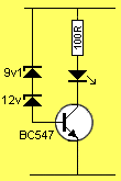
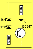
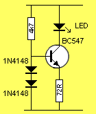
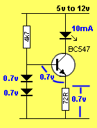 When
the circuit is turned ON, 0.7v will be developed across each diode.
When
the circuit is turned ON, 0.7v will be developed across each diode. 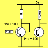
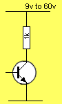
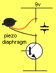
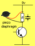
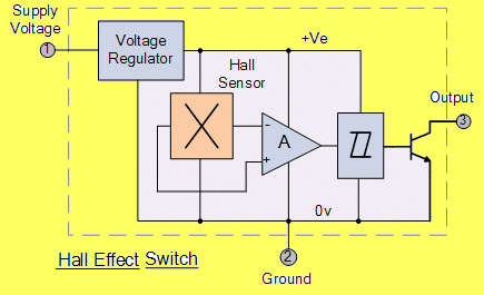
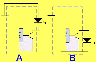
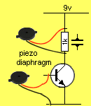
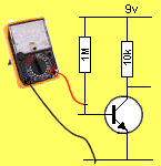
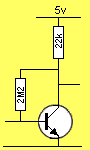
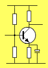
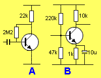
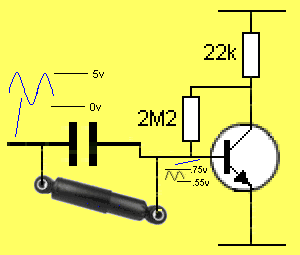
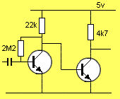
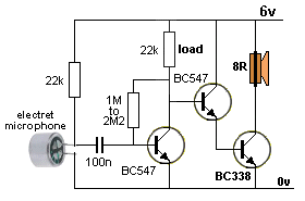
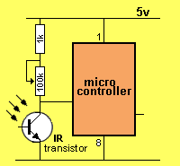
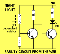
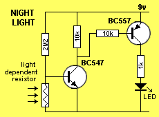
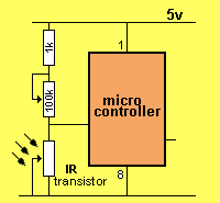
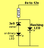
 23-12-2024